The University of Wisconsin-Madison electrical and computer engineering Professor Zhenqiang "Jack" Ma developed two imaging technologies sponsored by DoD.
With $750,000 in support from the Air Force Office of Scientific Research (AFOSR), Ma has developed curved night-vision goggles using germanium nanomembranes.
Creating night-vision goggles with a curved surface allows a wider field of view for pilots, but requires highly photosensitive materials with mechanical bendability-the silicon used in conventional image sensors doesn't cut it.
Instead, Ma's design employs flexible germanium nanomembranes: a transferrable flexible semiconductor that until now has been too challenging to use in imagers due to a high dark current, the background electrical current that flows through photosensitive materials even when they aren't exposed to light.
"Because of their higher dark current, the image often comes up much noisier on germanium-based imagers," says Ma. "We solved that problem."
Ma's dark current reduction technology has also been recently licensed to Intel.
In another imaging project, the U.S. Department of Defense has provided Ma with $750,000 in support of development of imagers for military surveillance that span multiple spectra, combining infrared and visible light into a single image.
Ma will employ a heterogeneous semiconductor nanomembrane, stacking the two incompatible materials in each pixel of the new imager to layer IR and visible images on top of one another in a single image.
The result will be imagers that can seamlessly shift between IR and visible images, allowing the picture to be richer and more quickly utilized for strategic decisionmaking.
"They are looking for the highest resolution they can get," says Ma. "Something that can take one picture with everything in it."
Saturday, December 29, 2012
Friday, December 28, 2012
Omnivision Applies for Hardmask Patent
Omnivision's patent application US20120319242 "Dopant implantation hardmask for forming doped isolation regions in image sensors" by Duli Mao, Hsin-Chih Tai, Vincent Venezia, Keh-Chiang Ku, Yin Qian, Gang Chen, Rongsheng Yang, Howard Rhodes talks about using hardmask for high-energy implants between PDs. The mentioned hardmask materials are silicon oxide and polysilicon. The application talks about openings of order of 0.2-0.4um with hardmask thickness of 2um, said to have enough stopping power for 1MeV boron implants (combined with photoresist).
I'm a little surprised to see that the application was filed only in June 2011; I thought Omnivision has been using hardmasks since much earlier than that.
I'm a little surprised to see that the application was filed only in June 2011; I thought Omnivision has been using hardmasks since much earlier than that.
Thursday, December 27, 2012
Toshiba Announces Light Field Camera Module
The Asahi Shimbun: Toshiba has developed a light field camera module that allow users to refocus any part of the photograph afterward, similar to Lytro camera.
The cube-shaped module is about 1 centimeter per side and contains a dense array of 500,000 lenses, each 30um in diameter, in front of an image sensor measuring 5 mm by 7 mm. Each lens captures a slightly different image from one another, and the camera is said to produce a large, complete picture by using original software to combine the 500,000 tiny images.

The new camera is said to be able to measure the distance to an object based on the differences among the small images. It can also create pictures that are focused on every single part of the image. The camera module can also be used to take videos, and allow the users to retain the image of a figure in the foreground while replacing the background.
Toshiba plans to commercialize the module by the end of fiscal 2013 (March 2014), and call on smartphone manufacturers and other companies to adopt the technology.
Toshiba provided the newspaper with the sample images showing the camera module's after-the-fact refocusing capabilities:
 |
| A picture refocused on a man on front |
 |
| A picture refocused on a man on far back |
TI Licenses Softkinetic's Technology, Enters ToF Market
PR Newswire: TI enters ToF 3D sensing market through licensing of Softkinetic's DepthSense pixel and sensor technology and iisu middleware for gesture recognition. TI opens a special web page devoted to its 3D ToF imaging solutions.
Mitch Reifel, Softkinetic's VP Sales, says: "TI has licensed SoftKinetic’s TOF pixel technology and has entered the TOF market with their own branded sensors (similar to an ARM licensing model). TI will also supply various chips around the sensor (power management, etc.) to provide a complete TOF system. The goal is obviously high-volume consumer electronics, where TI can leverage its large-scale manufacturing to bring down costs.
...we licensed our core pixel technology to TI, who will now manufacture and sell sensors (and support chips like a TOF controller) under their brand name.
...They will be combining this into a more integrated system over time (i.e. fewer chips), as well as adding other technology they have in the TI portfolio. Moving forward TI will provide a portfolio of sensors (they are announcing two so far with this announcement) and companies can go to TI for custom TOF chips, different array sizes, etc.
This model means that SoftKinetic is no longer a direct provider of TOF chips, but rather a technology licensing company for TOF technology."
"There are a plethora of applications that can benefit from the accuracy and resolution of this technology," said Gaurang Shah, VP of Audio and Imaging Products at TI. "Imagine an end equipment designer tilting, rotating, compressing and expanding a new product in 3D to inspect and evaluate it on their PC before committing to a hardware prototype. We believe our collaboration with SoftKinetic will ignite more applications like this, and foster further technology innovation to simplify the way we interact with machines."
So far the reference design from TI consists of:
TI compares 3D camera technologies:

At CES 2013 TI will demo its new 3D ToF image sensor chipset inside 3D cameras that control a laptop and a smart TV to access and navigate movies, games and other content with the wave of a hand. The TV demonstration also features TI's OMAP 5 processor, which powers a natural user interface with gesture recognition and full-HD graphics (Flash player required):
Mitch Reifel, Softkinetic's VP Sales, says: "TI has licensed SoftKinetic’s TOF pixel technology and has entered the TOF market with their own branded sensors (similar to an ARM licensing model). TI will also supply various chips around the sensor (power management, etc.) to provide a complete TOF system. The goal is obviously high-volume consumer electronics, where TI can leverage its large-scale manufacturing to bring down costs.
...we licensed our core pixel technology to TI, who will now manufacture and sell sensors (and support chips like a TOF controller) under their brand name.
...They will be combining this into a more integrated system over time (i.e. fewer chips), as well as adding other technology they have in the TI portfolio. Moving forward TI will provide a portfolio of sensors (they are announcing two so far with this announcement) and companies can go to TI for custom TOF chips, different array sizes, etc.
This model means that SoftKinetic is no longer a direct provider of TOF chips, but rather a technology licensing company for TOF technology."
"There are a plethora of applications that can benefit from the accuracy and resolution of this technology," said Gaurang Shah, VP of Audio and Imaging Products at TI. "Imagine an end equipment designer tilting, rotating, compressing and expanding a new product in 3D to inspect and evaluate it on their PC before committing to a hardware prototype. We believe our collaboration with SoftKinetic will ignite more applications like this, and foster further technology innovation to simplify the way we interact with machines."
So far the reference design from TI consists of:
- 3D Time of Flight (ToF) Sensors:
OPT8130 – QQVGA (160 x 120)
OPT8140 – QVGA (320 x 240) - VSP5324 – Analog Front End
- TFC – Time of Flight Controller
- Supporting Solutions:
Power Management
LED Driver
- OPT8130: 0.25 A/W at 870 nm
- OPT8140: 0.15 A/W at 850 nm
 |
| TI's 3D Time of Flight (ToF) Sensor Chipset Solution |
TI compares 3D camera technologies:

At CES 2013 TI will demo its new 3D ToF image sensor chipset inside 3D cameras that control a laptop and a smart TV to access and navigate movies, games and other content with the wave of a hand. The TV demonstration also features TI's OMAP 5 processor, which powers a natural user interface with gesture recognition and full-HD graphics (Flash player required):

Wednesday, December 26, 2012
Toshiba Announces 20MP/30fps Sensor, Aims to 30% Market Share
Business Wire: Toshiba announces a 20MP image sensor based on 1.2um BSI pixels, the TCM5115CL, aimed to DSC market and claimed to have the industry's highest resolution in 1/2.3-inch format. The new sensor is said to achieve a 15% improvement in full well capacity over Toshiba's previous generation 16MP sensor with pixel size of 1.34um. TCM5115CL delivers the high frame rates of 30fps at full 20MP resolution (10b RAW output), 60fps at 1080p and 100fps at 720p.
Sampling of the new sensor will begin at the end of January 2013 and mass production will follow in August 2013.
CMOS image sensors are declared to be the main product of Toshiba's Analog and Imaging System business. The company's target is to reach a 30% market share in 2015. The previous plan aimed to achieve that target in 2013.

Tuesday, December 25, 2012
Panavision Imaging Changes its Name to Dynamax Imaging
I'm not sure what it means, but Panavision Imaging web site now presents itself as Dynamax Imaging.
Update: I was told that Panavision Imaging has been sold on Dec. 18. Only about a half of the team got the offer to join the new company, the other half has been laid off. It's not clear who is the buyer. If somebody knows more details, please let us know.
Update: I was told that Panavision Imaging has been sold on Dec. 18. Only about a half of the team got the offer to join the new company, the other half has been laid off. It's not clear who is the buyer. If somebody knows more details, please let us know.
Saturday, December 22, 2012
DxOMark Over The Years and Generations
Luminous Landscape published a trend analysis of DxOMark sensor database by Peter van den Hamer. The analysis nicely demos a steady sensor performance improvement over the years. Some of the modern 1/1.7-inch and even 1/2.33-inch sensors reach the same aggregate score as DSLRs from 2003 - rather impressive progress.
Friday, December 21, 2012
Aptina's Two 8MP Sensors Feature 6MP/60fps Video Mode
Business Wire: Aptina launches two fast 8MP sensors for mobile devices and sports cameras. The AR0835 targets the mobile device market, while the AR0835HS is aimed to sports camera market for very fast cameras with still and video capabilities.
The new high-speed sensors enable the full-width 16:9 6MP video window to be readout at 60 fps without pixel binning or cropping the field-of-view. This 6MP data stream oversamples the target image by 3x resulting in video that is said to be as sharp as that of the high-end multi-sensor video cameras used in television studios. In addition, camera designers can take advantage of this speed to enable the capture of 6MP still images without interrupting the video stream and with zero shutter lag.
"Aptina’s advanced A-PixHS technology takes the 1.4-micron BSI pixel to the next level with a high speed architecture that provides uncompromised image quality and very fast frame rate video," said Roger Panicacci, VP of Product Development at Aptina.
The sensors’ other features include HDR capabilities in still and video modes; on-chip binning to provide 720p120; an optional on-chip scaler to reduce data transmission rates to enable operation with a wide range of image coprocessors, and slow-motion playback. Unique to the AR0835 mobile sensor is pin-to-pin compatibility along with a shared lens and lens placement to accommodate standard modules with Aptina’s 8MP AR0833. The video camera AR0835HS sensor uses a proprietary extremely fast (up to 32-lanes) HiSPi data interface while the AR0835 uses a 4-lane MIPI interface.
The AR0835 is in mass production now, available in both die form as a stand-alone sensor, and with Aptina’s mobile ISP for a fully tuned, complete camera solution. The AR0835HS is currently sampling in a new 10mm x 10mm CLCC package and will be available in mass production in Q1 2013.
The History of Black Silicon in Photodetector Patents
I got this paper by email. It has a lot of historical references and obscure and esoteric facts. While I do not agree with few points here, I think many might find this paper interesting:
----------
THE HISTORY OF “BLACK SILICON” IN PHOTODETECTOR PATENTS
Leonard Forbes*, Life Member IEEE
L. Forbes and Associates, LLC
PO Box 1716
Corvallis, OR 97339
lenforbes@forbes4.com
“Black silicon” is a semiconductor material, a surface modification of silicon with very low reflectance of visible and infrared light. The modification was discovered in the 1960’s as an unwanted side effect of chemical etching [1] and again in the 1980’s as an unwanted side effect of reactive ion etching. [2] Black silicon, or textured surfaces, can be inadvertently produced by any of a number of known chemical etches, and are to be avoided in integrated circuits. [3]
Unfortunately in the late 1990’s and 2000’s black silicon was again produced as an effect of laser ablation and etching and consequentially some magical photoelectric properties were claimed by Prof. Eric Mazur and his students a Harvard University. One of the best examples of this is the 2006 paper by J.E. Carey et al. claiming a very high photo-gain associated with “the high density of impurities and structural defects in the microstructured layer.” [4] It turns out in retrospect that the high gain was probably associated with a bulk silicon photoconductive effect as a result of annealing the high resistivity float zone, FZ, silicon substrates at 700C to 800C resulting in conversion of the substrate to even higher resistivities by the introduction of oxygen donors. By their own admission there was a long period of time they could not duplicate the photodetector effects, presumably they had unknowingly changed to Czochralski, CZ , substrates that are lower resistivity and for which it is more difficult to form high resistivity substrates. All the results in their journal article [4] can be explained as photoconductors on high resistivity bulk silicon substrates with poor contacts. Photoconductors can have a very high photogain. [6] The Harvard University and SiOnyx 2009 patent application [5] claimed a “photovoltaic effect” as well as the “high gain photodiodes.” Fig. 13 in their report supposedly demonstrating this photovoltaic effect has no photovoltage at zero current! By definition “photovoltaic” means some photovoltage develops under illumination of an open circuit connected semiconductor junction diode. It is also difficult to have “high gain photodiodes” unless you have some mechanism for carrier multiplication, but it is fairly easy to have high gain photoconductors [6], or even negative photoconductivity [7] !
Nature has been using the textured structures technology for probably millions of years. A moth’s eye has pillars on the surface of the eye, a texture, that reduces reflectance to one or two per cent. [8] In the case of tropical butterflies mother nature is even more clever, the textured surface on their wings reflects polarized light that only other butterflies can see, to predators the butterfly is a green against a green background.[9] The first human reference describing the textured structure and reduced reflectance as applicable to moths and applicable to solar cells is probably in 1935 by Von D. A. G. Bruggemann. [10] He described one mechanism for reduced reflectance, a lowering of the average index of refraction making possible the use of antireflecting layers, partly of silicon, partly of air. Antireflecting layers with a lower index of refraction than glass are commonly used in eye glasses. Another effect to reduce reflection on solar cells was a large pyramid texture resulting in multiple attempts at transmission into the silicon. Front side texturing of photodetectors to reduce reflectance and increase the scattering of light in the substrate was described by Arndt et al. of COMSAT in 1975. [11] Arndt described both the use of front side texture and antireflecting layers.
Backside textured surfaces for photdetectors were first described in the 1960’s. A.E. St. John described backside texturing of photodetectors in 1969[ 12 ] and these were again described in 1983 by Czubatyj et al. [13]. A.E. St John suggested a simple formulation for the enhancement of the absorption of weakly absorbed infrared light in silicon by the scattering of this light at the textured backside and increased path length for absorption. We just adapted and modified this using a simple assumption in our review article and analysis of solar cells.[ 14] Different textures for solar cells were widely investigated in the early 1980’s particularly by Yablonovitch [15] and also by Campbell and Green the latter at the UNSW in Australia. [16]
Given that CZ silicon samples as are conventionally used in silicon processing do not provide high gain photodetectors then the increased absorption of CZ silicon devices in the infrared, but without gain, is easily explained by texturing of the black silicon surfaces. The idea of laser texturing of silicon surfaces in photodetectors was reported by Russell et al. in 1992 [17] and then again in detail in 2003 [18]. Yamamoto et al. have described in detail the experimental results of backside texturing of photodetectors [19] by laser ablation and we provided a simple analysis of their results by backside scattering of light in photodetectors [14]. The net result is that all of the claimed phenomena for black silicon, reduced reflectance, increased absorption in the infrared as claimed by Mazur, Carey and the SiOnyx et al. can be explained by old phenomena commonly know to those skilled in the art of silicon technology. One skilled in the art will however soon appreciate that laser ablation introduces a huge number of defects and that it virtually impossible to anneal all of these out. These defects are particularly detrimental to photodetectors and solar cells so “black silicon” as described by Mazur, Carey, and SiOnyx et al. is simply not likely to be useful or employed in such devices demonstrating any utility. Textured devices produced by chemical etch, however, are useful and are commonly used in solar cells being sold commercially in the USA since before 2009.[20]
Recently there have been attempts to apply black silicon as the front side texture in solar cells, the first of these by the National Renewable Energy Lab., NREL, [21] used a porous silicon etch on the front side to reduce reflectance. However, while this works well in reducing the visible light reflectance of bare silicon wafers with no backside layers or materials from 46 % to a few % it is not clear that this provides any scattering of the light in the substrate. The texture comprises tall vertical structures, and 30% of the infrared light is still reflected. In a collaborative project NREL and Natcore developed the blackest of all black silicon, also known as the “Blackest Solar Cell” that absorbs 99.7% sunlight . A metal catalyzes used as a porous silicon etch creates millions of holes on the surface of a silicon wafer already having a large texture. Natcore provided the liquid phase deposited oxide to fill the holes for passivation of the surface. [22] Even more recently SiOnyx used laser ablation [23] to create a fine texture on the front side of solar cells that already had an ISO texture ( isotropic – acidic textured) wafers [24] but this made at best only a 0.3% improvement in conversion efficiency.
Texturing by chemical etch has also been previously disclosed for use in CMOS imagers. [25} However, the high density of defects introduced into the thin photodiodes by laser ablation [5] will result in a reduction in yield and increase in dark current and consequent loss of utility.
Patents are supposed to benefit the public. The Constitution implicitly expresses this intent, the US Patent Office acknowledges this, and the Supreme Court has so interpreted it. Yet the current patent system fails miserably short of realizing this purpose. One example of the system's failure is the absence of a timely, inexpensive mechanism for invalidating the high number of bad patents being issued. As a result of this void, the public is suffering, and enormous wastes of expenditures of investor and public funding are incurred. There is as demonstrated by the previous example of “black silicon” a dire need for reform. The recent change by the America Invents Act in allowing an easier mechanism for third party submissions during patent prosecution [26] is a first step in this direction.
_________________________________________________________________
* Leonard Forbes is a semi-retired Professor and is currently America’s most prolific living inventor in electrical sciences and technology.
References
[1] L. Forbes, unpublished thesis work, University of Illinois, 1968-1969 ;
c.f. for a historical review http://doc.utwente.nl/38679/1/t0000018.pdf
[2] H. Jansen, M. de Boer, R. Legtenberg, M. Elwenspoek, "The black silicon method: a universal method for determining the parameter setting of a fluorine-based reactive ion etcher in deep silicon trench etching with profile control,” Journal of Micromechanics and Microengineering , vol. 5, no. 2, p. 115. doi:10.1088/0960-1317/5/2/015
[3] United States Patent Application 20070167011 M. Hidaka July 19, 2007 “Etching method(to avoid forming black silicon).”
[4] Z. Huang, J.E. Carey, M. Liu, X. Guo, J. C. Campbell and E. Mazur, “Microstructured silicon photodetector,” Appl. Phys. Letters, vol. 89, 033506, 2006.
[5] US Patent Application Publication US 2010/0052088 J.E. Carey, X. Li, and N. J. McCaffrey Mar. 4, 2010 “High Sensitivity Photodetectors, Imaging arrays, and High Efficiency Photovoltaic Devices produced using Ion Implantation and Femtosecond Laser Irradiation,”
and also United States Patent 7,781,856 E. Mazur and J.E.Carey August 24, 2010
"Silicon-based visible and near-infrared optoelectric devices."
[6] S. M. Sze, “Physics of Semiconductor Devices.” Wiley Interscience, New York, 2nd Ed., 1981, p. 746.
[7] C-T. Sah, L. Forbes and W.W. Chan, "A New Model of Negative Photocurrent," Science Bulletin of National Chiao-Tung University, vol. V, no. 2, pp. 1-10, 1972.
[8] S. A. Boden and D. M. Bagnall, “Nanostructured Biomimetic Moth-eye Arrays in Silicon by Nanoimprint Lithography,” Proc. of SPIE, vol. 7401, 74010J, 2009. doi: 10.1117/12.826201
[9] The Times, London, UK, May 31, 2010 , “Bank Note Nanotechnology based on Butterfly Wings could beat Forgers.”
[10] Von D. A. G. Bruggemann , “Berechnung Verschiedcner Physikalischer Konstanten von Heterogenen Substanzen,” Annalen der Physik, 5. folge, band 24, pp. 636-664, Sept. 1935.
[11] R. A. Arndt, J. F. Allison, J. G. Haynos, and A. Meulenberg, Jr., “Optical properties of the COMSAT non-reflective cell,” 11th IEEE Photovoltaic Spec. Conf., pp. 40-43, 1975.
[12] United States Patent 3,487,223 A.E. St John 30 Dec. 1969 “Multiple Internal Reflection Structure in a Silicon (Photo)Detector which is Obtained by Sandblasting.”
[13] United States Patent 4,419,533 W. Czubatyj, R. Singh, J. Doehler, D.D. Allred, and J.M. Reyes Dec. 6, 1983 “Photovoltaic Device having Incident Radiation Directing means for Total Internal Reflection.”
[14] L. Forbes, “Texturing, reflectivity, diffuse scattering and light trapping in silicon solar cells,” Solar Energy, vol. 86, no. 1, pp. 319-325, Jan. 2012, doi: 10.1016/j.solener.2011.10.003
[15] E. Yablonovich, and G.D. Cody, “Intensity Enhancement in Textured Optical Sheets for Solar Cells,” IEEE Transactions on Electron Devices, vol. ED-29, pp. 300-305, 1982.
[16] P. Campbell and M. A. Green, “High performance light trapping textures for monocrystalline silicon solar cells,” doi: 10.1016/S0927-0248(00)00115-X
[17] United States Patent 5,164,324 S.D. Russell, D. A. Sexton and E.P. Kelley Nov. 17, 1992 “Laser Texturing.”
[18] S. D. Russell, A. D. Ramirez, and E. P. Kelley, “Nanosecond Excimer Laser Processing for Novel Microelectronic Fabrication,” ie SSC Pacific Technical Reports , vol. 4 Navigation and Applied Sciences, pp. 228-233, 2003. http://www.spawar.navy.mil/sti/publications/pubs/td/3155/5a_S4papers/NanoXLaser.pdf
[19] K. Yamamoto, A. Sakamoto, T. Nagano, and K. Fukumitsu, “NIR sensitivity enhancement by laser treatment for Si detectors,” Nuclear Instr. and Meth. Phys., vol. A624, pp. 520-523, 2010.
[20] Z. Shi, S. Wenham, J. Ji, S. Partlin, and A. Sugianto, “Mass Production of the Innovative Pluto Solar Cell Technology,” SunTech, White paper , 2011. http://am.suntech-power.com/
[21] H.-C. Yuan, V. E. Yost, M. R. Page, P. Stradins, D. L. Meier and H. M. Branz, “Efficient black silicon solar cell with a density-graded nanoporous surface: Optical properties, performance limitations, and design rules,” Appl. Phys. Lett., vol. 95, 123501, 2009. doi:10.1063/1.3231438
[22] United States Patent 6,080,683 Maria Faur, Mircea Faur, D. Flood, S.G. Bailey and Horia M. Faur June 27, 2000
“Room temperature wet chemical growth process of SiO based oxides on silicon.”
[23] C. Vineis, M. Levy-Finklshtein, J. Carey, G. Knight, E. Wefringhaus and R. Harney, “Ultrafast Laser Texturing for Enhanced Solar Cell Performance and Lower Cost,”
http://www. sionyx.com/pdf/solarcellperformancewhitepaper.pdf
[24] T. Geipel, S. Pingel, J. Dittrich, Y. Zemen, G. Kropke, M. Wittner, and J. Berghold,
“Comparison of acidic and alkaline textured multicrystalline solar cells in a solar panel production,” http://www.solon.com/export/sites/default/solonse.com/_downloads/global/article-pid/Geipel_et_al_texturization.pdf
[25] United States Patent 7,456,452 D. Wells and S. P. Leiphart Nov. 25,2008
“Light sensor having undulating features for CMOS imager.”
[26] http://www.gpo.gov/fdsys/pkg/FR-2012-07-17/pdf/2012-16710.pdf
Thursday, December 20, 2012
SMIC Announces BSI Test Chip Success
PRNewswire: SMIC, China's largest and most advanced semiconductor foundry, announced it has a BSI CMOS image sensor "first test chip demonstrating good image quality even in low-light conditions". The complete BSI process has been independently developed by SMIC and is targeted to enter risk production with partnering customers in 2013.
While driving its BSI technology toward commercial production, the company is soon to begin early development of next-generation CIS technology based on 3D integrated circuits.
"We are proud to be the first Chinese foundry to successfully develop BSI CMOS image sensors," said SMIC CEO Dr. TY Chiu. "CMOS image sensors are among the key value-added technologies that SMIC offers for customers in the mobile device and imaging markets."
"With this achievement as a stepping stone, our development team will drive the BSI sensor technology to timely commercialization," added Dr. Shiuh-Wuu Lee , SMIC's SVP of Technology Development. "This breakthrough further solidifies SMIC's position as the advanced technology leader in China."
Since the introduction of its FSI CIS process in 2005, SMIC has become a major CIS foundry in China, primarily for mobile phone and consumer electronics applications. In order to provide turnkey CIS fabrication service, SMIC and Toppan Printing of Japan operate a joint venture, Toppan SMIC Electronics (Shanghai) Co., Ltd., (TSES), which fabricates on-chip color filters and micro lenses at SMIC's Shanghai site.
Wednesday, December 19, 2012
PMD Demos Low-Latency Interface
A new PMD CamBoard video on Youtube demos extremely low latency (there are sequences recorded in 4x and 8x slow motion), good ambient light performance and efficient switching from low power mode to active mode. PMD combines it with face recognition to validate that a user is looking towards the screen to minimize the risk of unintended usage: An interaction is only possible if a face has been detected and a valid finger pose is observed.
Tuesday, December 18, 2012
Apple Applies for HDR Imaging Patent, Looks for Highly Innovative Sensor Engineers
Apple applies for US2012/041398 (US20120314100) patent titled "Image Sensor Having HDR Capture Capability" by Michael Frank.
"...there exist disadvantages to the process of generating a HDR image from multiple independently captured images. For example, changes may occur when images are captured successively such that a composite HDR image generated therefrom may not be completely aligned. This may generate motion artifacts in the composite HDR image. Further, the images may be affected by local motion in the image scene, e.g., trees swaying in the wind, people and faces shifting slightly, etc. Additionally, the time required for a HDR image to be processed may be delayed based on the images to be captured."
So, the solution is to read same row several times, each time with different exposure. Then the several reads are combined into a single HDR row in an image processor:


"To generate a HDR image during a single exposure of the frame (i.e., fixed amount of time t during which the rolling shutter reset 80 moves across a frame), multiple reads of the same row of pixels of the image sensor may occur. For example, a first data read 86, of the data stored in a row of pixels, may be undertaken at a time n, where n is a fixed fractional time of time t. This time n may be, for example, 1/2, 1/3, 1/4, 1/5, 1/10, 1/20, or another value of the frame time t. This time n may be represented as line 88 in FIG. 5. That is, the first data read 86 may occur at a time n subsequent to the reset of a row of pixels by the rolling shutter reset 80.
Accordingly, as the rolling shutter reset 80 passes downwards along line 78, the first data read 86 may trail the rolling shutter reset 80 by time n. In this manner, data stored in the pixels for each row of the frame may be read at a time n after the rolling shutter reset 80 of that row of pixels. Thus, each row of pixels read as the first data read 86 passes across the image sensor will have been exposed to light for the same time n, which may be referred to as an exposure time or integration time."
While the exact reference escapes me, I've heard about a similar technique being used by a major security camera vendor for more than 10 years now. It might be new in a smartphone world though.
While we are at Apple, Terry Gilton, Senior Director of Sensor Technology at Apple, posted a note on his LinkedIn page:
"I am seeking some more ultra-motivated, highly innovative sensor engineers. Some opportunities in characterization, validation, analog design, and architecture of all kinds of sensors. If you are passionate about sensing stuff and feel like you want to change the world, let me know."
Monday, December 17, 2012
Image Sensors 2013 Program
Image Sensors 2013 conference speaker list is finalized. The conference is to be held on March 19-21 in London, UK. There is quite a lot of good presentations in the list, possibly, even exceeding the previous years:
There are also unnamed presentations by Rico Marchesi, VP Sales & Marketing, EPSROS PHOTONICS, Switzerland and Chris Yates, CTO, ODOS IMAGING, UK.
Thanks to RS for sending me the info!
- BSI CMOS Image Sensors with RGBC Technology
Dr Howard E Rhodes, CTO, OMNIVISION, USA - SPADnet: Smart Sensor Network with Embedded Coincidence Detection for PET applications
Prof Edoardo Charbon, TU DELFT, The Netherlands - Broadcast Global Shuttered Low Noise CMOS Imagers
Dr.Ir Peter Centen, Director R&D, BU Cameras, GRASS VALLEY, The Netherlands - Silicon MEMS Auto Focus Camera Modules
Dr Alexandru Drimbarean, Sr. Director, Research & Development, DIGITALOPTICS CORPORATION, UK - SPAD-based Time-of-Flight sensor for mobile/consumer applications
Marc Drader, ST MICROELECTRONICS, UK - Past, present and future of DSC technology and image quality
Dietmar Wueller, Director, IMAGE ENGINEERING, Germany - Optimising sCMOS sensor performance in digital camera applications
Dr Gerhard Holst, Head of R&D, PCO, Germany - Will emerging technologies and new applications reshape the CMOS image sensors industry?
Paul Danini, Technology & Market Analyst, Imaging Technologies & MEMS Devices, YOLE DEVELOPPEMENT, France - Long-Range Time-of-Flight Imaging in CMOS for Advanced Driving-Assistance Systems
Dr Cristiano Niclass, Researcher, TOYOTA CENTRAL R&D LABS, Japan - Update on MISPiA project - CMOS SPAD imagers at the single-photon level, for 2D imaging and 3D ranging acquisitions
Prof Franco Zappa, POLIMI, Italy - What’s wrong with the modern DSC – a maverick colour scientist’s view on areas for improvement
Alan Roberts, Colour Science Consultant (former BBC R&D), UK - Mythbusting 3D imaging – where this sector is really heading
Jim Lewis, CEO, MESA IMAGING, Switzerland - Exploring the duality of image sensor and display technology development in 3D broadcast technology – experiences from the London 2012 Olympics and beyond..
Jim De Filippis, Broadcast Engineering Consultant, FOX TV, USA - Multi Aperture Imaging – why? And why now?
Ziv Attar, CEO and Co Founder, LINX IMAGING, Israel - A Thin Form Factor, High Resolution, and High Performance Camera Array Architecture for Mobile Imaging
Kartik Venkataraman, Founder and CTO, PELICAN IMAGING, USA - High-resolution, High-Frame Rate CMOS Image Sensors for High-End DSC/DVC Applications
Junichi Nakamura, Managing Director, CMOS Image Sensor Design Center, APTINA, Japan - Very Large Area CMOS Imagers for Healthcare
Professor Nigel M Allinson, MBE, Distinguished Chair of Image Engineering Lincoln School of Computer Science, UNIVERSITY OF LINCOLN, UK
There are also unnamed presentations by Rico Marchesi, VP Sales & Marketing, EPSROS PHOTONICS, Switzerland and Chris Yates, CTO, ODOS IMAGING, UK.
Thanks to RS for sending me the info!
Friday, December 14, 2012
Sony Vintage CCD Uses Non-Bayer CFA
EE Video Blog's Youtube video teardown of 1985 Sony CCD-V8AF-E 8mm video camera reveals that its CCD uses non-Bayer color filter. So, it appears that Sony F65, ClearVid and other non-bayer CFAs for video applications have a long tradition. I wonder if CMYG video sensors too had many different versions in production.
 |
| Microscope image of the Sony 1985 CFA |
Wednesday, December 12, 2012
Learning ISP Self-Adapts to Various Color Filter Patterns
Stanford University applied for a patent US20120307116 "Learning of image processing pipeline for digital imaging devices" by Steven Lansel and Brian Wandell.
Abstract: "A learning technique is provided that learns how to process images by exploiting the spatial and spectral correlations inherent in image data to process and enhance images. Using a training set of input and desired output images, regression coefficients are learned that are optimal for a predefined estimation function that estimates the values at a pixel of the desired output image using a collection of similarly located pixels in the input image. Application of the learned regression coefficients is fast, robust to noise, adapts to the particulars of a dataset, and generalizes to a large variety of applications. The invention enables the use of image sensors with novel color filter array designs that offer expanded capabilities beyond existing sensors and take advantage of typical high pixel counts."

Abstract: "A learning technique is provided that learns how to process images by exploiting the spatial and spectral correlations inherent in image data to process and enhance images. Using a training set of input and desired output images, regression coefficients are learned that are optimal for a predefined estimation function that estimates the values at a pixel of the desired output image using a collection of similarly located pixels in the input image. Application of the learned regression coefficients is fast, robust to noise, adapts to the particulars of a dataset, and generalizes to a large variety of applications. The invention enables the use of image sensors with novel color filter array designs that offer expanded capabilities beyond existing sensors and take advantage of typical high pixel counts."

Tuesday, December 11, 2012
Superpix and Galaxycore Recognized for Best Tech Support in China
PR Newswire: EETimes-China 11th Annual China Fabless Survey revealed that Galaxycore and Superpix are among Top 10 Outstanding Technical Support companies. Superpix made it for the second year in a row (see last year results). Galaxycore also won "2012 Forbes China Best Potential Enterprise Award".
Talking about China-based CIS companies, recently Superpix announced its first 1.75um pixel design - the 2MP SP2518. Galaxycore announced its second generation 1.75um pixel sensor the GC2015. The first generation one was announced a year ago.
Meanwhile, the third China's image sensor company, Brigates, launches its first sensor targeting high end security cameras, the MCCD-BG0601. Its IR sensitivity is said to be 3 times of that of CCDs. The D1 (PAL) resolution sensor uses 8.3um x 8.6um pixels.

Update: Credit Suisse report from Nov. 15 gives some more data about Galaxycore sales, #4 in China's biggest fabless companies list:
"In the CMOS image sensor market, SMIC’s key customer – GalaxyCore (private) – shipped around 600 mn units in 2011, an increase of 70% from 350 mn units in 2010. The majority of GalaxyCore’s CIS has resolution is under 2Mpixels and it mainly serves the China feature phone market and is preparing for higher-pixel products for the booming smartphone market."

Primesense to Unveil New, More Compact 3D Camera
PR Newswire: Primesense announces its next generation embedded 3D sensor, Capri, demonstrating a small form factor and low cost. The new reference design utilizes Capri - PrimeSense's next-generation of depth acquisition SoC, with improved algorithms including multi-modal 3D sensing techniques. Its thin form factor is aimed to embedding in consumer electronics devices such as PCs, All –in-One PCs, tablets, laptops, mobile phones, TVs, consumer robotics and more.
"Using cutting-edge technologies, our newest generation of sensors is robust, accurate and affordable," said Inon Beracha, CEO, PrimeSense. "With a mind-blowing size reduction, Capri's size is about x10 smaller than the PrimeSense's current generation of 3D sensors and it is certainly the smallest 3D sensor in the world. Capri is small enough to fit into today's most popular Smartphones while still providing the highest depth performance (short and long range). We see Capri adding depth sensing and Natural Interaction to numerous devices and markets, revolutionizing the user experience and usability in ways that no one could imagine until now".
Samples for development and integration for OEMs will be available by mid-2013.
Monday, December 10, 2012
CIS Process is One of the Three ST's Manufacturing Pillars
EETimes: ST announces its restructuring strategy. When asked about manufacturing strategy, ST CEO Carlo Bozotti told analysts there is a three-legged manufacturing strategy for Crolles, all fundamental for the future of the company.
One of the legs is CIS process – a part of ST's business that had been under a strategic review in 2010. At that time it had been decided to adopt a policy of application diversification and that this has been successful, Bozotti said. ST has multiple design wins in automotive and elsewhere, he added.
The other two legs are embedded non-volatile memory and FDSOI processes.
Toshiba Announces 5MP 1.4um SoC
Toshiba announces 5MP 1.4um pixel sensor with integrated ISP, the T4K39. The 1/4-inch sensor is intended for use in camera phones.

Saturday, December 08, 2012
Playing Fruit Ninja with PMD Camera
PMD published an Youtube demo of Fruit Ninja game controlled by its Camboard Nano and Omek Interactive's middleware. The game is quite dynamic, both speed and delay are important, so it's quite impressive demo:
Friday, December 07, 2012
Panasonic Proposes Color-Based 3D Imager
Panasonic patent application US20120293634 "Three-dimensional imaging device" by Yasunori Ishii and Masao Hiramoto proposes to use color mask in the lens to get color shift-based parallax information and determine the distance to the objects:


e2v Keeps Working on EM CMOS Sensor
After the first patent application on electron multiplying CMOS sensor e2v applies for another patent, the US20120292483 "Electron-multiplication image sensor" by Pierre Fereyre, Frédéric Mayer. The multiplication is achieved by repeating 4B-4E sequence many times:


Thursday, December 06, 2012
NEC Shrinks IR Pixel to Less Than Wavelength Size
Tech-On: NEC has developed an uncooled VGA IR sensor with pixel pitch of 12um. The sensor operates in 8-14um band, so its pixel size is less than one wavelength. The pixel is based on NEC's own MEMS technology.

Wednesday, December 05, 2012
Progress in pH Imager-Based Genome Sequencing
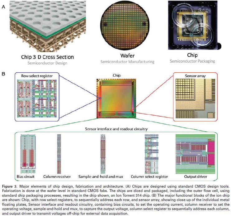
Electrophoresis journal published "Progress in Ion Torrent semiconductor chip based sequencing" paper by Barry Merriman, Ion Torrent R&D Team, Jonathan M. Rothberg, where Ion Torrent team includes over 300 people. The paper represents the collective work of the Ion Torrent R&D Team over the past three years:
"In order for next-generation sequencing to become widely used as a diagnostic in the healthcare industry, sequencing instrumentation will need to be mass produced with a high degree of quality and economy. One way to achieve this is to recast DNA sequencing in a format that fully leverages the manufacturing base created for computer chips, complementary metal-oxide semiconductor chip fabrication, which is the current pinnacle of large scale, high quality, low-cost manufacturing of high technology. To achieve this, ideally the entire sensory apparatus of the sequencer would be embodied in a standard semiconductor chip, manufactured in the same fab facilities used for logic and memory chips. Recently, such a sequencing chip, and the associated sequencing platform, has been developed and commercialized by Ion Torrent, a division of Life Technologies, Inc. Here we provide an overview of this semiconductor chip based sequencing technology, and summarize the progress made since its commercial introduction. We described in detail the progress in chip scaling, sequencing throughput, read length, and accuracy. We also summarize the enhancements in the associated platform, including sample preparation, data processing, and engagement of the broader development community through open source and crowdsourcing initiatives."

The progress of pH sensors is quite similar to image sensors: the resolution has grown from 1.5MP to 165MP (!), while pixel pitch has shrunk from 5.1um to 1.68um leveraging process scaling from 0.35um to 0.11um. Everything looks familiar, except the price is much higher than that of image sensors, see the last comment to the previous post on Ion Torrent.
Thanks to VZ for the link!
"In order for next-generation sequencing to become widely used as a diagnostic in the healthcare industry, sequencing instrumentation will need to be mass produced with a high degree of quality and economy. One way to achieve this is to recast DNA sequencing in a format that fully leverages the manufacturing base created for computer chips, complementary metal-oxide semiconductor chip fabrication, which is the current pinnacle of large scale, high quality, low-cost manufacturing of high technology. To achieve this, ideally the entire sensory apparatus of the sequencer would be embodied in a standard semiconductor chip, manufactured in the same fab facilities used for logic and memory chips. Recently, such a sequencing chip, and the associated sequencing platform, has been developed and commercialized by Ion Torrent, a division of Life Technologies, Inc. Here we provide an overview of this semiconductor chip based sequencing technology, and summarize the progress made since its commercial introduction. We described in detail the progress in chip scaling, sequencing throughput, read length, and accuracy. We also summarize the enhancements in the associated platform, including sample preparation, data processing, and engagement of the broader development community through open source and crowdsourcing initiatives."
The progress of pH sensors is quite similar to image sensors: the resolution has grown from 1.5MP to 165MP (!), while pixel pitch has shrunk from 5.1um to 1.68um leveraging process scaling from 0.35um to 0.11um. Everything looks familiar, except the price is much higher than that of image sensors, see the last comment to the previous post on Ion Torrent.
Thanks to VZ for the link!
Genpla 3D Camera and Gesture Recognition
This Youtube video presents Korea-based Genpla 3D camera and gesture recognition. The camera seems to be based on stereo principle:


Tuesday, December 04, 2012
News from France: Sofradir Buys Thales and Sagem IR Sensor Facilities
Sofradir acquires Sagem and Thales’ IR detector technology development and manufacturing facilities. Under the agreement, Sagem will transfer to Sofradir the Indium Antimonide (InSb) technology. The Quantum Well-Infrared Photodetector (QWIP) and Indium Gallium Arsenide (InGaAs) technologies will be transferred to Sofradir from the GIE III-V Lab, an economic interest group with partners Alcatel Lucent, Thales and CEA.
By consolidating these IR technologies under one roof, Sofradir joins a small circle of IR detector manufacturers with expertise in all the cooled and uncooled IR technologies. Sofradir is currently ranked number one for volume deliveries of IR detectors based on its Mercury Cadmium Telluride (HgCdTe) technology.
"The technologies from Sagem and the III-V Lab enable Sofradir to have from this point forward the complete portfolio of infrared technologies," said Philippe Bensussan, chairman and CEO of Sofradir. "With the new technologies, Sofradir, along with its subsidiary ULIS, will be able to select the technology best adapted to our clients’ applications."
NXP Annouces H.264 IP Security Camera Processor
Marketwire: NXP announces ASC884xA and ASC885xA series of single-chip video processors for HD IP security cameras. These devices integrate virtually all functions required for an IP camera design -- from raw image sensor data input, ISP, and H.264 compression, to secure encrypted transmission over the network through a Gigabit Ethernet interface.
Capturing 60 frames per second at Full HD resolution (1080p/60), the new series supports H.264 High Profile encoding while consuming less than 1.5 W of power, said to be the best power efficiency and lowest bit rate compared to other solutions on the market today. Further, the ASC884xA and ASC885xA devices incorporate very flexible spatial and temporal (2D/3D) noise reduction for excellent low-light performance.
In addition to ASC8852A flagship product for 1080p/60 performance, NXP is releasing a complete range of pin-compatible Advanced ICs down to 1080p/30 (ASC8850A) and 720p/30 (ASC8848A). The ASC8848A offers an H.264-encoded bit rate of less than 500 kbit/s at a power consumption level close to 0.5 W. Evaluation samples of the ASC8848A, ASC8849A, ASC8850A, ASC8851A and ASC8852A will be available to lead customers starting in Q1 2013, with volume manufacturing starting in Q2 2013.
Sony is the 2nd Best Performing Semiconductor Company in Top 20 List
IHS iSuppli report on top 20 semiconductor companies says about Sony performance:
"After Qualcomm, the next best performance among the Top 20 suppliers is set to be posted by Sony, which will attain 20.1 percent growth in semiconductor revenue. Sony's performance stands in stark contrast to most other major Japanese semiconductor suppliers, whose revenue will collapse by double-digit rates in 2012."
"Sony's strong results are due to its leading position in the image sensor market, which is expected to grow by 19 percent in 2012, with the CMOS image sensor sector of the market seeing its revenue expand by 31.8 percent. Sony's image sensor revenue, which accounts for nearly 60 percent of its semiconductor takings, is expected to expand by 48 percent. Even more amazing, its CMOS image sensor revenues are forecast to more than double," says Dale Ford, iSuppli's analyst.

Invisage Selected as a 2012 Red Herring Top 100 Global Company
Marketwire: InVisage announces that it is a recipient of the Red Herring Top 100 Global award, recognizing the leading private companies from North America, Europe, and Asia.
"This prestigious award reinforces the huge impact our image sensors with QuantumFilm technology will have on the industry at large," said Jess Lee, president and CEO of InVisage. "We appreciate the recognition, and are proud to be part of such an esteemed list of companies."
Update: Invisage web site went through a major redesign and now its technology page shows a small-scale sample image dated by June 28, 2012:

Toshiba Enters Automotive Imaging Market
PR Newswire: Toshiba announces its first image sensor for the automotive and security/surveillance markets, a 1/4-inch TCM5114PL VGA sensor with HDR and fast frame rates.
"Toshiba is leveraging its industry-leading CMOS imaging technology into new markets with stellar results," said Andrew Burt, vice president of the Analog and Imaging Business Unit, System LSI Group at TAEC. "The low-power consumption, and rich imagery enabled by this device in various light conditions will appeal to manufacturers in the automotive industry."
The TCM5114PL sensor delivers DR of 100dB at 60 fps at VGA resolution. The sensor is based on 5.6um pixel with > 6V/lx.s senstivity and has integrated ISP and HDR functions. The TCM5114PL has both a digital and analog (NTSC/PAL) interface so it can connect to currently available display panels. The device supports YUV422/RGB565/ RGB888/ RAW10/RAW12 data formats.
Samples of the TCM5114PL VGA image sensor are currently available. Mass production is scheduled for March 2013. Sample pricing is set at $25.

Saturday, December 01, 2012
Raytrix Presentation at VISION 2012 Show
A 15 min long Vimeo Raytrix presentation at VISION 2012 shows the new effects and once again explains the principle of lightfield camera:
A pdf version of the presentation is here. Youtube version of the video is here.
A pdf version of the presentation is here. Youtube version of the video is here.
Sony Production Capacity
The latest Sony semiconductor business summary sheet dated by Nov. 27, 2012 says that the company's production capacity is 40M units per month for CMOS sensors and 12M units a month for CCDs. The main image sensor fabs are:
- Nagasaki TEC (CMOS Sensors)
- Kagoshima TEC (CCDs)
- Kumamoto TEC (CCD&CMOS Sensors)
- Sony Device Technology (Thailand) Co., Ltd. (CCD&CMOS Sensor assembly)
Friday, November 30, 2012
IISW 2013 Final Call for Papers
2013 International Image Sensor Workshop (IISW), to be held on Snowbird Resort, Utah, USA, June 12-16, 2013, published a Final Call for Papers:
The scope of the workshop includes all aspects of electronic image sensor design and
development. In addition to regular papers, the workshop will include invited talks, poster presentations, discussion sessions, and Walter Kosonocky Award. Extra time has been added to permit longer discussion and more informal meeting time.
Papers on the following topics are solicited:
Image Sensor Design and Performance
Pixels and Image Sensor Device Physics
Application Specific Imagers
Fabrication and testing
Submission of papers: Abstracts should be submitted electronically to the Technical Program Chair, Gennadiy Agranov (see email in the pdf on IISW site). The deadline for abstracts submission is January 23, 2013.
The scope of the workshop includes all aspects of electronic image sensor design and
development. In addition to regular papers, the workshop will include invited talks, poster presentations, discussion sessions, and Walter Kosonocky Award. Extra time has been added to permit longer discussion and more informal meeting time.
Papers on the following topics are solicited:
Image Sensor Design and Performance
- CMOS Image sensors, CCD and CID image sensors. New architectures.
- Image sensors with rolling shutter and global shutter.
- Image sensors architecture, Low noise readout circuitry, ADC designs
- High frame rate Image sensors, High dynamic range sensors, Low voltage and low power
- High image quality. Low noise. High sensitivity. High color reproduction.
- Non-standard color patterns with special digital processing
- System-on-a-chip, Image sensors with digital preprocessing
Pixels and Image Sensor Device Physics
- New devices and structures. Advanced materials.
- Small pixels development, testing, and characterization
- New device physics and phenomena
- Techniques for increasing QE, well capacity, reducing crosstalk, and improving angular performance
- Front side illuminated and back side illuminated pixels and pixel arrays
- Nanotechnologies for Imaging
- Pixel simulation: Optical and Electrical simulation, 2D and 3D, CAD for design and simulation.
Application Specific Imagers
- Image sensors and pixels for depth sensing: TOF, RGBZ, Structured light, etc.
- Image sensors with enhanced spectral sensitivity (NIR, UV)
- Pixels and Image sensors for stereo Imaging
- Sensors for DVC, DSC, Mobile, DSLR and mirror-less cameras
- Array Imagers and sensors for Computational Imaging
- Sensors for medical applications, microbiology, genome sequencing,
- High energy photon and particle sensors (X-ray, Radiation).
Fabrication and testing
- New fabrication techniques. Backside thinning. Scaling.
- Wafer stacking, multilayer sensors, “3D” integration
- Advanced optical path, Color filters. Microlens. Light guide
- Packaging and Testing. Wafer level cameras
- Reliability. Yield. Cost.
- Defects. Leakage current. Radiation damage.
Submission of papers: Abstracts should be submitted electronically to the Technical Program Chair, Gennadiy Agranov (see email in the pdf on IISW site). The deadline for abstracts submission is January 23, 2013.
8MP Stacked Sensor, 12MP Power and Speed Marvel and More From Sony
Sony Cx-News vol. 70 is entirely devoted to new and very impressive image sensor announcements. The first of the two most interesting ones is 1.55um BSI pixel-based IMX117CQT. This 1/2.3-inch 12.4MP sensor is an improvement on the similar but older IMX078CQK. The new sensor is faster, lower power, has wider light acceptance angle, and more:


The sensor is very fast delivering 35fps at full resolution at 430mW power. It also capable to 4K/60fps video (10b ADC mode) and includes HD-ish slow motion modes:

Another important announcement is the first stacked sensor product, the 1/4-inch 8MP 1.12um pixel ISX014, naturally, with integrated ISP:
Not much information is given about the sensor. It supports 1940 x 1080p video at 30fps and 1280 x 720p video at 60fps. The built-in scalar function makes it possible to shrink all of the 8MP to perform 16:9 cropping for video. Power consumption is 270 mW in 8MP JPEG@15fps mode or 202 mW in 2MP YUV@30mode which are quite good numbers, possibly due to an advanced process node used for ISP die.
The image samples which were supposed to show the sensor's high quality, are of low resolution, unfortunately:

Another announcement is the new 1-inch 9.19MP CCDs: the ICX814ALG (B&W) and the ICX814AQG (color). The sensors have 4 outputs and multitude of readout modes, the fastest one being 1080p at 36fps:
The sensor is very fast delivering 35fps at full resolution at 430mW power. It also capable to 4K/60fps video (10b ADC mode) and includes HD-ish slow motion modes:

Another important announcement is the first stacked sensor product, the 1/4-inch 8MP 1.12um pixel ISX014, naturally, with integrated ISP:
 |
| Sony illustration of the stacked structure does not seem to have any wafer-to-wafer contacts in the pixel array area |
Not much information is given about the sensor. It supports 1940 x 1080p video at 30fps and 1280 x 720p video at 60fps. The built-in scalar function makes it possible to shrink all of the 8MP to perform 16:9 cropping for video. Power consumption is 270 mW in 8MP JPEG@15fps mode or 202 mW in 2MP YUV@30mode which are quite good numbers, possibly due to an advanced process node used for ISP die.
The image samples which were supposed to show the sensor's high quality, are of low resolution, unfortunately:

Another announcement is the new 1-inch 9.19MP CCDs: the ICX814ALG (B&W) and the ICX814AQG (color). The sensors have 4 outputs and multitude of readout modes, the fastest one being 1080p at 36fps:
Thursday, November 29, 2012
Raymond Wu Re-Joins Omnivision
PR Newswire: Omnivision reported its quarterly results on the higher end of its guidance: $390.1M, as compared to $258.1M in the previous quarter, and $217.9M a year ago. GAAP net income $10.3M, as compared to $2.3M in the previous quarter, and $21.1M a year ago.
GAAP gross margin is 16.6%, as compared to 19.1% in the previous quarter and 30.6% a year ago. The sequential decrease was attributed to an increase in shipment mix of advanced products that carried high manufacturing costs.
"In addition, I am pleased to announce the addition of Raymond Wu to OmniVision's management team," said Shaw Hong, Omnivision's CEO. "Raymond, one of our co-founders, has agreed to re-join us as our President, effective December 1, 2012. During his previous tenure, Raymond's intellect, experience and influence extended to market development, engineering and sales. We are enthused by his return, and with his knowledge of our company and the industry, I expect Raymond to make significant contributions to OmniVision's continued growth in the years to come."
Raymond Wu used to be Omnivision's EVP and left the company in August 2006.
Update: SeekingAlpha published Omnivision's earnings call transcript with more details on its business.
PMD and Mesa ToF Cameras Comparison
Open access Remote Sensing journal published a nice paper comparing PMD's CamCube3.0 and Mesa Imaging's SR-4000 ToF cameras and also giving a nice background on other ToF solutions:
SR-4000 and CamCube3.0 Time of Flight (ToF) Cameras: Tests and Comparison
Dario Piatti and Fulvio Rinaudo
DITAG, Politecnico di Torino, Torino, Italy
The paper starts with a nice table filled with parameters of many ToF cameras, both historical and available now on the market:
The influence of camera warm-up on distance measurement is analyzed: a warm-up of 40 minutes is suggested to obtain the measurement stability, especially in the case of the PMD's CamCube3.0. Depth accuracy tests have shown similar numbers of of order of millimeters for both cameras.
Via Vision Systems Design.
SR-4000 and CamCube3.0 Time of Flight (ToF) Cameras: Tests and Comparison
Dario Piatti and Fulvio Rinaudo
DITAG, Politecnico di Torino, Torino, Italy
The paper starts with a nice table filled with parameters of many ToF cameras, both historical and available now on the market:

The influence of camera warm-up on distance measurement is analyzed: a warm-up of 40 minutes is suggested to obtain the measurement stability, especially in the case of the PMD's CamCube3.0. Depth accuracy tests have shown similar numbers of of order of millimeters for both cameras.
 |
| Mesa's SR-4000 is on the left, PMD's CamCube3.0 on the right. Question mark means the accuracy has not been measured yet. |
Via Vision Systems Design.
Pansonic Presents its SmartFSI at IDW 2012
International Display Workshops combined with Asia Display 2012 to be held in Kyoto, Japan on December 4-7, has few image sensor presentations. For the first time Panasonic openly presents its SmartFSI technology:
Evolution of Eyes and Image Sensors
H. Watanabe
Panasonic, Japan
The evolution of the eye and image sensors was overviewed. The possible disadvantage of the inverted structures of human eyes and FSI image sensors was solved with the use of the lightpipe function. A novel “SmartFSI” image sensor with stacked lightpipe structure demonstrated a high performance.
There are quite a few other interesting presentations, including 3 by Samsung:
A 1.5 Mpixel RGBZ CMOS Image Sensor for User Interface and 3D Image Capture
W. Kim, J. Yun, S.-H. Lee, Y. Wang, I. Ovsiannikov, Y. Park, C. Chung
Samsung, Korea, USA
A 1.5 Mpixel RGBZ image sensor to capture color (RGB) and depth (Z) at the same time is presented. Time-Of-Flight (TOF) method is used for depth. Color pixels and depth pixels are placed together in pixel array with specially designed RGBZ pattern. It demonstrates excellent depth performance and full color image.
A Full-HD CMOS Image Sensor with TimeMultiplexed 2D/3D Image Acquisition
S.-J. Kim, J. Shin, J. D. K. Kim, B. Kang, K. Lee
Samsung Advanced Inst. of Tech., Korea
We present a 1920x1080 pixel array to provide high-resolution 2D color images and high-accuracy 3D depth maps in a time-multiplexed manner. The prototype chip demonstrates the demodulation of 20 MHz time-of-flight signal with the contrast of 52.8%, achieving less than 38 mm depth error between the distance of 0.75 m and 4.5 m. [For a good multi-purpose gesture recognition one needs less than 10mm accuracy - ISW]
Amorphous Oxide Semiconductor Thin Film Transistor for Novel Device Applications
S. Jeon, I. Song, S.-E. Ahn, C. I. Kim, U.-I. Chung
Samsung Advanced Inst. of Tech., Samsung Elect., Korea
Among various semiconductor devices, electronically active oxide thin film transistors (TFTs) have received considerable attention for a wide range of device applications. In this presentation, we review various device applications utilizing amorphous oxide semiconductor TFT, which include photo-sensor, image sensor and other device applications.
Low Noise Readout Circuits Interface Using a Capacitive-Feedback Frontend Amplifier for High Output Impedance Sensors
K. Mars, S. Kawahito
Shizuoka Univ., Japan
In this paper a low-noise high-gain readout circuit interface for high output impedance sensors is presented. Theoretical noise analysis and simulation results shows that by using a high-gain switched capacitor amplifier, the thermal noise is greatly reduced if the dominant reset noise component at the charge summing node is canceled.
An Ultra-Low Voltage CMOS Imager with Novel Pulse-Width-Modulation Readout
C.-C. Hsieh, M.-T. Chung
Nat. Tsing Hua Univ., Taiwan
A 0.5 V PWM CMOS Imager chip with threshold variation cancelling and programmable threshold control scheme was implemented. It achieves 0.055% pixel FPN, 0.65 LSBrms random noise at dark, and 82 dB dynamic range at 11.8 fps. The chip consumes 4.95 µW at 11.8 fps; results in a iFOM as 163.9 pW/f-p.
Discussing Pixel Circuits for Hybrid Sensor and Display Pixel Arrays
N. Papadopoulos, M. Yang, M. Esmaeili-Rad, M. Sachdev, W. S. Wong
Univ. of Waterloo, Canada
The hybrid sensor and display pixel proposed consists of: light sensor and integrated display onto the backplane. Phototransistors incorporating both sensing and switching on the same device was used. The backplane was implemented using a driving TFT and an OLED. The grey scale is generated by pulse-height and width voltage modulation.
Report from Symposium on Microoptical Imaging and Projection, Part 3
Albert Theuwissen concludes his series of reports by the discussion of poLight AF technology presented at the Symposium.
More Leap and PMD Demos
Leap Motion added 4 more video demos to its third-party developers playlist, so that the list currently has 7 videos. Most of the new videos demo gesture control in games.
Meanwhile PMD too published the finger tracking demo running on its CamBoard nano platform:
Meanwhile PMD too published the finger tracking demo running on its CamBoard nano platform:
Advantest Upgraded its CIS Tester Speed
Advantest introduces what it claims to be the industry's fastest image-capture module to cost-efficiently test image sensors with D-PHY and M-PHY interfaces. The new T2000 3Gbps CMOS Image Capture Module operates on its T2000 ISS system:
The T2000 3Gbps CMOS Image Capture Module simultaneously tests up to 64 devices in parallel, significantly reducing test costs. In addition to improving yields by performing at-speed testing in production, the module also can be used to shorten turnaround time in verifying semiconductor designs on first silicon.

"Ongoing, rapid improvements in the performance and resolution of CMOS image sensors as well as the growing volume of electronic products depending upon them continue to exert downward pressure on production costs," said Satoru Nagumo, senior vice president of the ASD Test Business Group at Advantest Corporation. "Our newest generation of image-capturing technology enables our customers to lower the cost of test while meeting the performance requirements for advanced image sensors."
The T2000 3Gbps CMOS Image Capture Module simultaneously tests up to 64 devices in parallel, significantly reducing test costs. In addition to improving yields by performing at-speed testing in production, the module also can be used to shorten turnaround time in verifying semiconductor designs on first silicon.
"Ongoing, rapid improvements in the performance and resolution of CMOS image sensors as well as the growing volume of electronic products depending upon them continue to exert downward pressure on production costs," said Satoru Nagumo, senior vice president of the ASD Test Business Group at Advantest Corporation. "Our newest generation of image-capturing technology enables our customers to lower the cost of test while meeting the performance requirements for advanced image sensors."
Wednesday, November 28, 2012
Toshiba Announces 1.12um BSI Sensor with Improved SNR
PR Newswire: Toshiba announces a 13MP, 1.12um pixel sensor claimed to deliver high-image quality equivalent to a 1.4um pixel. The new T4K37 feature BSI and integrated color noise reduction (CNR) and fits into an 8.5mm x 8.5mm size camera module.
The miniaturization of pixel size impacts performance of light sensitivity and SNR in today's 1.12um pixel image sensors. BSI technology helps improve sensitivity, but is said to fall short on elevating image quality. Toshiba developed its newest image sensor with BSI and CNR integrated on the sensor to address both low-light sensitivity and SNR. As a result, the Toshiba CMOS image sensor provides approximately 1.5 times higher SNR than a 1.12um pixel sensor with no CNR.
Samples of the new Toshiba sensor, the T4K37, will be available in December 2012. Sample pricing begins at $20.00.

Update: It appears that Japanese PR has much more info. Among the pictures, it shows the CNR effect:
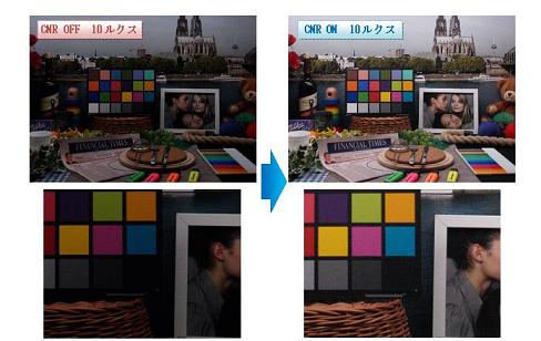
Here is the Google translation of CNR principle:
"CNR Our circuit has adopted the type to compare the image between frames by a digital filter circuit to suppress the color noise, without compromising a sense of resolution, of 1.12 micrometer pixel circuit not installed CNR SN ratio of about 1.5 times to accomplish, to achieve the SN ratio of the pixel corresponding to 1.4 micrometers."
The sensor is fast, it delivers 30fps at full 13MP resolution. The Japanese PR also has a table with two other sensors, apparently based on the same 1.12um pixel:

Update: Toshiba published a product page of the 1/3.07-inch T4K37 sensor. The block diagram shows a location of Color Noise Reduction part (CNR). The output format is either 8b or 10b.

The miniaturization of pixel size impacts performance of light sensitivity and SNR in today's 1.12um pixel image sensors. BSI technology helps improve sensitivity, but is said to fall short on elevating image quality. Toshiba developed its newest image sensor with BSI and CNR integrated on the sensor to address both low-light sensitivity and SNR. As a result, the Toshiba CMOS image sensor provides approximately 1.5 times higher SNR than a 1.12um pixel sensor with no CNR.
Samples of the new Toshiba sensor, the T4K37, will be available in December 2012. Sample pricing begins at $20.00.

Update: It appears that Japanese PR has much more info. Among the pictures, it shows the CNR effect:
Here is the Google translation of CNR principle:
"CNR Our circuit has adopted the type to compare the image between frames by a digital filter circuit to suppress the color noise, without compromising a sense of resolution, of 1.12 micrometer pixel circuit not installed CNR SN ratio of about 1.5 times to accomplish, to achieve the SN ratio of the pixel corresponding to 1.4 micrometers."
The sensor is fast, it delivers 30fps at full 13MP resolution. The Japanese PR also has a table with two other sensors, apparently based on the same 1.12um pixel:

Update: Toshiba published a product page of the 1/3.07-inch T4K37 sensor. The block diagram shows a location of Color Noise Reduction part (CNR). The output format is either 8b or 10b.
Continuation of Report from Symposium on Microoptical Imaging and Projection
Albert Theuwissen continues his notes from the Fraunhofer Symposium in Jena, Germany. The second part covers Heptagon wafer level optics and a prototype multi-aperture camera, talks about Lytro news and technical details, Fraunhofer in-house CIS process, Nemotec wafer scale optics, ST pixel simulations, and more.
Tuesday, November 27, 2012
Report from Symposium on Microoptical Imaging and Projection
Albert Theuwissen published a first part of his report from Symposium on Microoptical Imaging and Projection being held these days in Fraunhofer Institute, Jena, Germany. The first part of the report talks about multi-aperture imaging presented by Pelican Imaging, LinX, Ascentia, Fraunhofer and Onera.
ON Semi and Teledyne Designed 16MP MCT Sensor
Business Wire: ON Semiconductor collaborated with Teledyne Imaging Sensors to manufacture an Extremely Large Stitched Read Out Integrated Circuit (ELS ROIC) for astronomy.
The 16MP H4RG-15 consists of Teledyne’s HgCdTe detector material hybridized to a CMOS readout circuit. It is said to be the largest sensor ever produced for IR astronomy. The H4RG-15 63 mm x 63 mm stitched CMOS ROIC uses ON Semiconductor’s proprietary 180nm process. The ROIC is so large that only four die fit onto a 200 mm wafer.
The H4RG-15 ROICs were manufactured at ON Semiconductor’s fab located in Gresham, Oregon. With this project, ON Semiconductor has demonstrated that it can successfully produce the H4RG-15 with the yield required for this next generation sensor.
The H4RG-15 sensor has been installed at the University of Hawaii’s observatory on Mauna Kea to confirm the performance of the sensor under telescope observing conditions. "The resolution with which images can be captured using this new sensor system represents a major step forward in the progression of IR astronomy," said Dr. Donald Hall of the Institute for Astronomy at the University of Hawaii, who is the principal investigator for the NSF-funded H4RG-15 development program.
Saturday, November 24, 2012
Samsung S5K3H5 CMOS Sensor Promo
Samsung published a Youtube promo of its 8MP, 1.4um pixel S5K3H5 sensor promo. The sensor is used in Samsung Galaxy S3 smartphone. The video goes through the sensor spec with the video illustrations in the background. Another feature of the video is the 1.9MP 1/6-inch 1.75um pixel front sensor S5K6A3:
Friday, November 23, 2012
Leap Motion's Demos on Youtube
There are few new Leap Motion's gesture control videos appeared on Youtube. The videos are from different third party developers that Leap Motion kindly collected into a single playlist.
The first one shows finger recognition in action. The room is quite dark, hopefully it's not a system limitation:
The Quadrotor control works quite nicely. A delay is noticeable but it might come from mechanical stuff:
The pong game gesture control is shown in dark room too:
The first one shows finger recognition in action. The room is quite dark, hopefully it's not a system limitation:
The Quadrotor control works quite nicely. A delay is noticeable but it might come from mechanical stuff:
The pong game gesture control is shown in dark room too:
Thursday, November 22, 2012
IS2013 Publishes Confirmed Speakers List
Image Sensors 2013 conference to be held on March 19-21, 2013 in London, UK, published an impressive list of confirmed speakers:
- Dr Howard E Rhodes, CTO, OmniVision, USA
- Prof Franco Zappa, PoliMI, Italy
- Dr G Humpston, Director of Applications (Europe), Digital Optics Corporation, UK
- Dr.Ir Peter Centen, Director R&D, BU Cameras Grass Valley, The Netherlands
- Prof Edoardo Charbon, TU Delft, The Netherlands
- Paul Danini, Technology & Market Analyst, Imaging Technologies & Mems Devices, Yole Developpement, France
- Dietmar Wueller, Director, Image Engineering, Germany
- Dr Gerhard Holst, Head of R&D, PCO, Germany
ST Proposes LDO Regulator with Distributed Output Stage
ST patent application US20120286135 "Low drop-out regulator with distributed output network" by Jingfeng Gong, Yann Desprez-Le-Goarant (Singapore), proposed a regulator for a pixel array with distributed output transistor that "improves localized heat dissipation by spatially-distributing transistors, and reduces IR drop across an output track by providing a consistent output voltage at each output node located along the output track." (I'd say with improved consistency, not exactly the same voltages).
The prior art is shown on Fig. 1A:

The proposed solution is shown on Fig. 2:

The prior art is shown on Fig. 1A:

The proposed solution is shown on Fig. 2:

Wednesday, November 21, 2012
DALSA Wins Netherlands-Canadian Chamber of Commerce’s Business of the Year Award
Teledyne DALSA has been honored as Business of the Year by the Netherlands-Canadian Chamber of Commerce (NCCC). The NCCC’s annual award is presented to Canadian companies with a subsidiary in the Netherlands or to Dutch companies active in Canada.
The selection committee noted the success of Teledyne DALSA’s Netherlands-based Professional Imaging division. Located in the High Tech Campus in Eindhoven, which has been called “the smartest square kilometer in Europe” by Fortune magazine, the division developing large format image sensors and medical x-ray detectors.
"We are delighted and humbled to accept this honor," commented Dr. Edwin Roks, EVP and Managing Director of Teledyne DALSA’s Eindhoven operations. "None of our innovation happens in isolation. The collaboration between our groups in Canada and in The Netherlands is extremely important for us. I would like to thank the embassy and the NCCC for their role in facilitating transatlantic cooperation, and we will strive to continue this valuable, productive relationship."
Bryce Bayer Died
Imaging Resource: Bryce Bayer, the Eastman Kodak scientist who invented the almost standard color filter pattern that bears his name, has passed away. Bayer, 83, died on November 13th in Bath, Maine. The Bayer Filter array was patented in 1976, U.S. Patent No. 3,971,065. Bayer is also known for his recursively defined matrix used in ordered dithering.

Update: SR kindly sent me a photo of Bryce Bayer's notebook describing his RGB pattern idea for the first time:

Update: SR kindly sent me a photo of Bryce Bayer's notebook describing his RGB pattern idea for the first time:

Tuesday, November 20, 2012
Sharp Designs its Own CMOS Sensors
Sharp has been mostly known by its CCDs. The 2012 Sharp Components Catalog does not even mention CMOS sensors as a product category. However, one the the Oct. 2012 Cadence success stories reveals that "Recently Sharp embarked on designing a new consumer electronics CMOS image sensor."
"Cadence helped us achieve our target in the highly competitive arena of CMOS image sensors,” says Naoya Fujita, GM of Product Planning, Electronic Components and Devices Group, Sharp. "We were able to deliver the highest quality of silicon and get to market significantly faster than would have been possible with our previous flow. We exceeded our design requirements and expectations, and look forward to continued collaboration with Cadence to meet the growing demand for high-quality CMOS images sensors."

"Cadence helped us achieve our target in the highly competitive arena of CMOS image sensors,” says Naoya Fujita, GM of Product Planning, Electronic Components and Devices Group, Sharp. "We were able to deliver the highest quality of silicon and get to market significantly faster than would have been possible with our previous flow. We exceeded our design requirements and expectations, and look forward to continued collaboration with Cadence to meet the growing demand for high-quality CMOS images sensors."

Monday, November 19, 2012
ASIC for Large Format NIR/SWIR Imager Project Started
EETimes: A consortium formed by the Caeleste, Belgium, Easics, Belgium and SELEX Galileo, UK won the European Space Agency's call for tender AO/1-6814 Development of Prototype ASIC for Large Format NIR/SWIR Detector Array. The ASIC is targeted for use in future Space Science and Earth Observation missions. The 18 month development aims to design an ASIC dedicated to large format cryogenic NIR/SWIR Detector. The project has several challenging features:
The project will benefit from the experience of each consortium partner. Caeleste is responsible for the project supervision and the design of the analog section. Easics is designing the digital section using IMEC standard DARE library for radiation hardness. Easics is also in charge of the test system development. SELEX Galileo joins as IR/cryogenic expert and will provide support for cryogenic operation, test and evaluation.
Following the successful completion of this demonstrator phase, an industrialized version will be envisaged, aiming at providing such flexible and standard ASIC to European Companies willing to simplify the design of infrared instruments for space application.

Thanks to BD for sending me the news!
- 77K operation temperature
- Radiation hardness
- Fully programmable sequencer on chip
- 16bits analog to digital conversion chain
The project will benefit from the experience of each consortium partner. Caeleste is responsible for the project supervision and the design of the analog section. Easics is designing the digital section using IMEC standard DARE library for radiation hardness. Easics is also in charge of the test system development. SELEX Galileo joins as IR/cryogenic expert and will provide support for cryogenic operation, test and evaluation.
Following the successful completion of this demonstrator phase, an industrialized version will be envisaged, aiming at providing such flexible and standard ASIC to European Companies willing to simplify the design of infrared instruments for space application.

Thanks to BD for sending me the news!
Image Sensors at ISSCC 2013
ISSCC 2013 published its advance program with many image sensor papers, including Sony stacked sensor presentation:
A 1/4-inch 8Mpixel Back-Illuminated Stacked CMOS Image Sensor
S. Sukegawa, T. Umebayashi, T. Nakajima, H. Kawanobe, K. Koseki, I. Hirota, T. Haruta, M. Kasai, K. Fukumoto, T. Wakano, K. Inoue, H. Takahashi, T. Nagano, Y. Nitta, T. Hirayama, N. Fukushima
Sony, Atsugi, Japan;
Sony LSI Design, Atsugi, Japan
Sony Semiconductor, Kumamoto, Japan
A 3.4µW CMOS Image Sensor with Embedded Feature-Extraction Algorithm for Motion-Triggered Object-of-Interest Imaging
J. Choi, S. Park, J. Cho, E. Yoon, University of Michigan, Ann Arbor, MI
A 467nW CMOS Visual Motion Sensor with Temporal Averaging and Pixel Aggregation
G. Kim, M. Barangi, Z. Foo, N. Pinckney, S. Bang, D. Blaauw, D. Sylvester University of Michigan, Ann Arbor, MI
A Rolling-Shutter Distortion-Free 3D Stacked Image Sensor with -160dB Parasitic Light Sensitivity In-Pixel Storage Node
J. Aoki, Y. Takemoto, K. Kobayashi, N. Sakaguchi, M. Tsukimura, N. Takazawa, H. Kato, T. Kondo, H. Saito, Y. Gomi, Y. Tadaki, Olympus, Hachioji, Japan
An 8×16-pixel 92kSPAD Time-Resolved Sensor with On-Pixel 64ps 12b TDC and 100MS/s Real-Time Energy Histogramming in 0.13µm CIS Technology for PET/MRI Applications
L. H. Braga, L. Gasparini, L. Grant, R. K. Henderson, N. Massari, M. Perenzoni, D. Stoppa, R. Walker
Fondazione Bruno Kessler, Trento, Italy
STMicroelectronics, Edinburgh, UK
University of Edinburgh, Edinburgh, UK
A 0.18µm CMOS SoC for a 100m-Range 10fps 200×96-Pixel Time-of-Flight Depth Sensor
C. Niclass, M. Soga, H. Matsubara, M. Ogawa, M. Kagami
Toyota Central R&D Labs, Nagakute, Japan
3D Camera Based on Linear-Mode Gain-Modulated Avalanche Photodiodes
O. Shcherbakova, L. Pancheri, G-F. Dalla Betta, N. Massari, D. Stoppa
University of Trento, Trento, Italy.
Fondazione Bruno Kessler, Trento, Italy
A 3D Vision 2.1Mpixel Image Sensor for Single-Lens Camera Systems
S. Koyama, K. Onozawa, K. Tanaka, Y. Kato
Panasonic, Nagaokakyo, Japan
A 187.5µVrms-Read-Noise 51mW 1.4Mpixel CMOS Image Sensor with PMOSCAP Column CDS and 10b Self-Differential Offset-Cancelled Pipeline SAR-ADC
J. Deguchi, F. Tachibana, M. Morimoto, M. Chiba, T. Miyaba, H. Tanaka, K. Takenaka, S. Funayama, K. Amano, K. Sugiura, R. Okamoto, S. Kousai
Toshiba, Kawasaki, Japan;
Toshiba Microelectronics, Kawasaki, Japan
A 94GHz 3D-Image Radar Engine with 4TX/4RX Beamforming Scan Technique in 65nm CMOS
P-N. Chen, P-J. Peng, C. Kao, Y-L. Chen, J. Lee
National Taiwan University, Taipei, Taiwan
A [10°C ; 70°C] 640×480 17µm Pixel Pitch TEC-Less IR Bolometer Imager with Below 50mK and Below 4V Power Supply
B. Dupont, A. Dupret, S. Becker, A. Hamelin, F. Guellec, P. Imperinetti, W. Rabaud
CEA-LETI-MINATEC, Grenoble, France
The conference's forums include F4 Scientific Imaging forum having few nice overview presentations:
Overview of Scientific Imaging in the Frequency Range from X-Rays to Terahertz
Valérie Nguyen, CEA Leti MINATEC, Grenoble, France
Multispectral Imaging: When CMOS Does the Trick!
Matteo Perenzoni, Fondazione Bruno Kessler, Torento, Italy
Ultra-High-Speed Imaging
Shigetoshi Sugawa, Tohoku University, Sendai, Japan
Single-Photon Imaging with SPADs
Robert Henderson, University of Edinburgh, Edinburgh, UK
State-of-the-Art in Uncooled IR Sensors and Readout Circuitry
Patrick Robert, ULIS, Veurey-Voroize, France
High-Sensitivity Astronomical-Imaging Arrays with Cryogenic Electronics for Terahertz Waves
Hiroshi Matsuo, National Observatory of Japan, Tokyo, Japan
THz Imaging: What You See and What You Don’t!
Peter H. Siegel, Caltech/JPL, Pasedena, CA
Advanced Microwave Imaging Based on Modern Semiconductor Technologies
Sherif-Sayed Ahmed, Rohde & Schwarz, Munich, Germany
THz CMOS Image Sensors Using Schottky Barrier Diodes for Lensless Portable Applications
Kenneth O, University of Texas at Dallas, Dallas, TX
Subscribe to:
Posts (Atom)