Sunday, November 30, 2014
Paul Lee Elevated to IEEE Fellow
Paul Lee, ex-Kodak engineer, now with Exelis Geospatial Systems, Amityville, NY, has been elevated to IEEE Fellow Members "for contributions to the development of CMOS image sensor technology and the pinned photo-diode active pixel sensor." US5625210 patent "Active pixel sensor integrated with a pinned photodiode" by Paul Lee, Robert Guidash, Teh-Hsuang Lee, and Eric Stevens is one of Kodak's classics, and, quite possibly, the most often referred image sensor patent.
Silicon Nanowires in Image Sensors
Harward University published PhD Thesis "Vertical Silicon Nanowires for Image Sensor Applications" by Hyunsung Park. The thesis proposes to use Si nanowires of different diameter to create color filters. Oval wires can be used as polarization filters.


Thursday, November 27, 2014
ESPROS Announces BSI ToF Imager
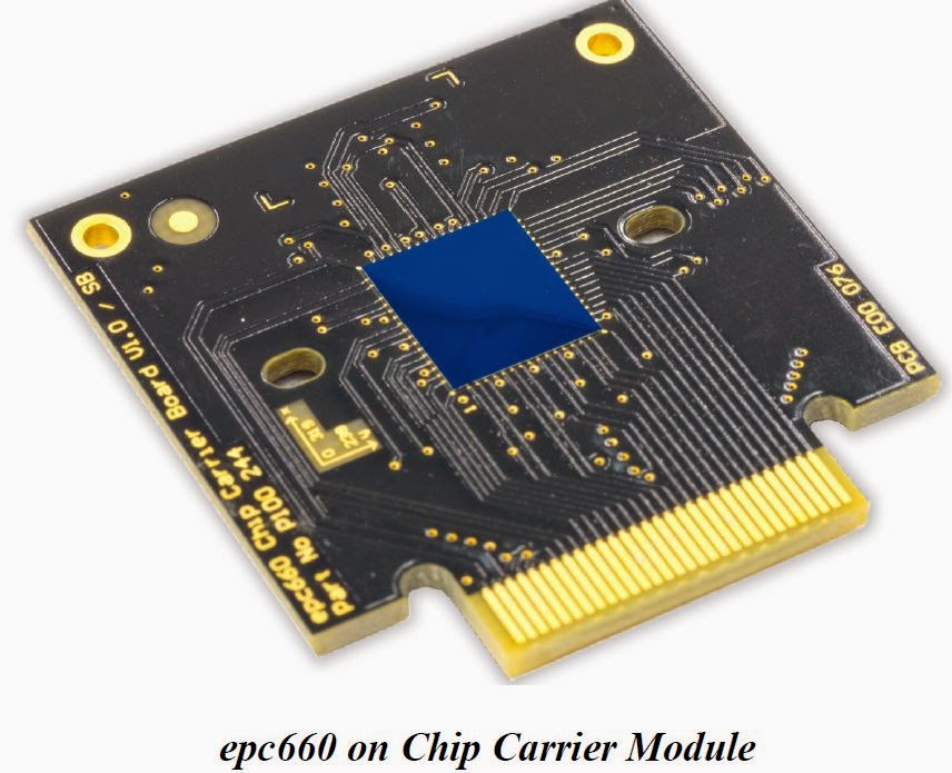
ESPROS announces epc660, a BSI 3D-TOF imager with a resolution of 320 x 240 pixels. epc660 is an integrated SoC combining high-QE BSI CCD pixel array and complete control logic to operate the device, an integrated LED driver, capable of driving more than 200mA peak current, and a high-speed 12-bit parallel video interface. The sensor speed is 66 TOF frames per second at QVGA resolution or up to 1000fps in "advanced operation modes." The advanced CCD pixel architecture is said to be the enabler for camera systems that can tolerate ambient light levels of up to 130Klux. Depending on the system design, a resolution in the millimeter range for distances up to 100 meters is said to be possible.
The epc660 features various modulation schemes on-chip, such as frequency hopping, random modulation, and CSMA/CD. There is also a dedicated modulation input that can be externally fed with any desired modulation signal.
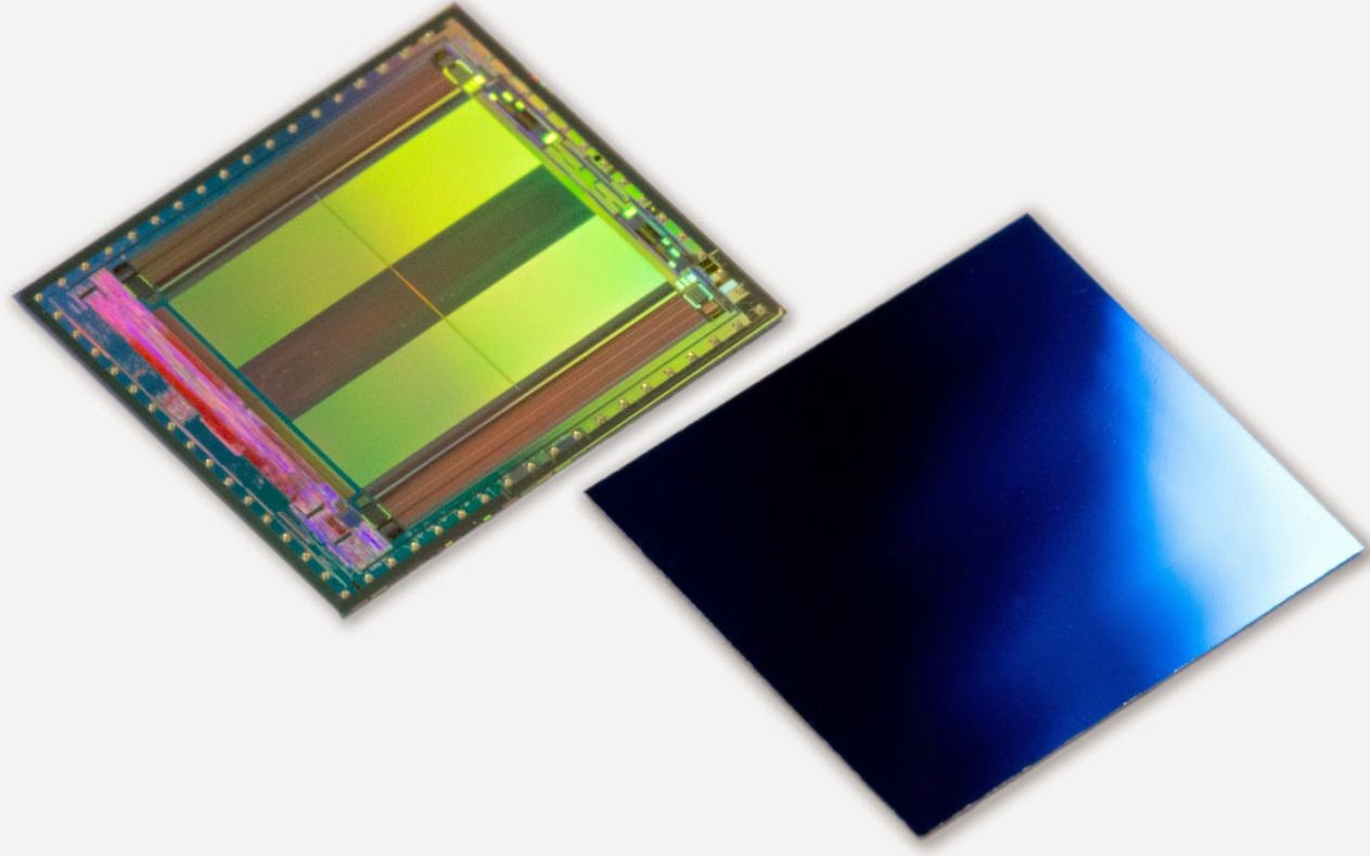
Source: ESPROS Nov. 2014 newsletter.
The epc660 features various modulation schemes on-chip, such as frequency hopping, random modulation, and CSMA/CD. There is also a dedicated modulation input that can be externally fed with any desired modulation signal.
Source: ESPROS Nov. 2014 newsletter.
Wednesday, November 26, 2014
World's Smallest Thermal Camera
Norvegian-language TU Industry reports that Prox Dynamics' PD-100 world's smallest military grade UAV is equipped by the smallest to-date FLIR thermal camera weighting just 0.5 gram. A few months ago their smallest camera was 25 grams. The unit which is mounted in the PD 100 T weighs half a gram, says CTO and Prox Dynamics Entrepreneur Petter Muren. The whole drone with visible and thermal cameras weighs just 17.5g:

Thanks to SO for the link!
Thanks to SO for the link!
Tuesday, November 25, 2014
Sony Achievements and Plans
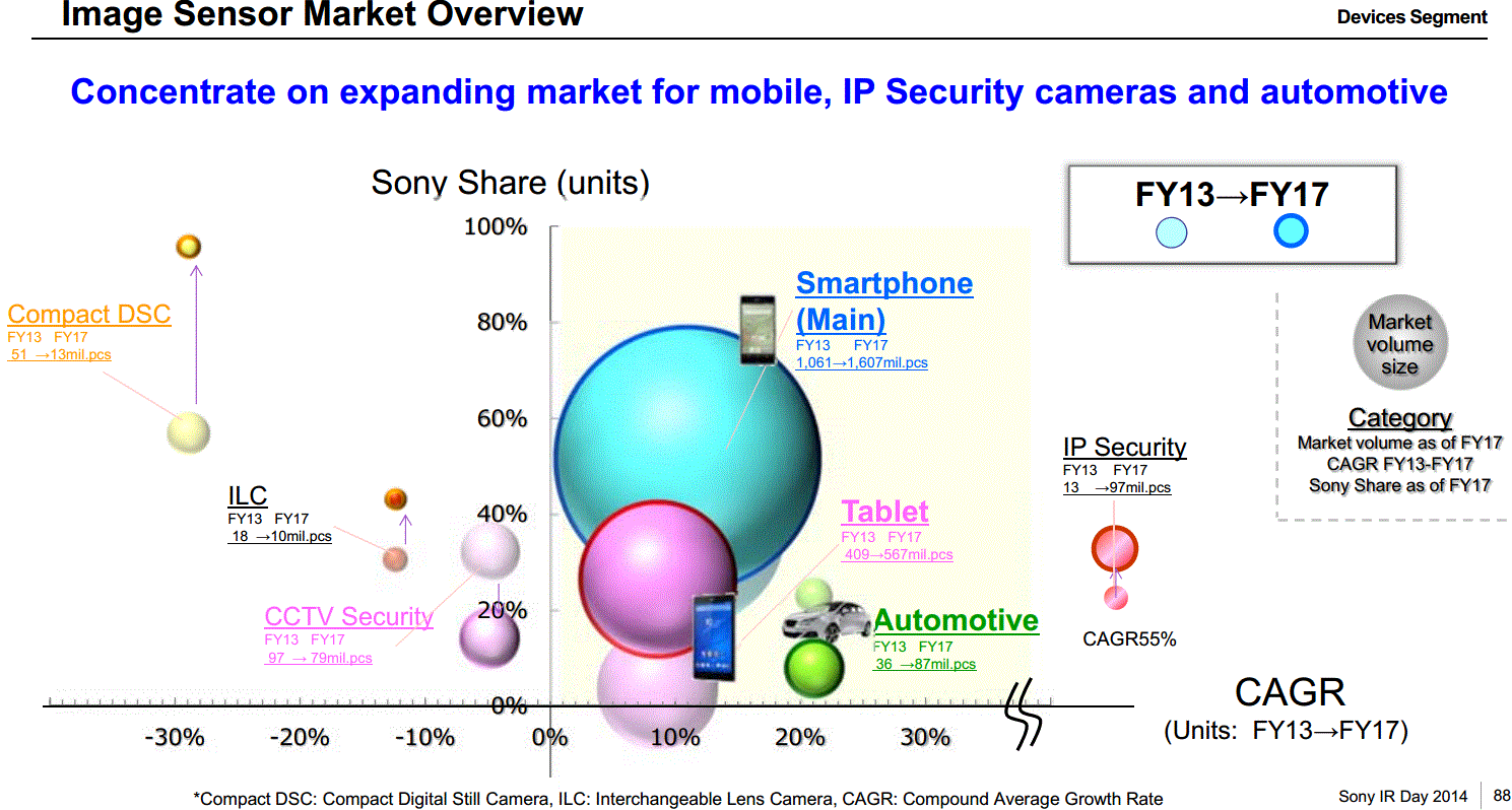
Sony has held an 2014 investor day today in Tokyo. Sony devices business presentation, shows impressive achievements and ambitious plans for a 3-year future:


Samsung Samples 1.0um Pixel Products
Samsung has held Investors Forum 2014 on Nov. 17 in NYC. Image sensor business update includes sampling of 1.0um pixel sensor:

Saturday, November 22, 2014
Gestigon Completes Series A Round
Lübeck, Germany-based gesture recognition company Gestigon announces it has closed a Series A funding round with a 7-digit-USD financing 10 days ago. The company has been founded in 2011 as a University of Lübeck spin-off, and now employs 21 people in offices in Lübeck, Germany and Sunnyvale, CA.
Gartner's 2014 Hype Cycle for Emerging Technologies maps gesture control as a maturing up technology with its plateau of productivity to be reached in the next 2-5 years:

Gartner's 2014 Hype Cycle for Emerging Technologies maps gesture control as a maturing up technology with its plateau of productivity to be reached in the next 2-5 years:
Friday, November 21, 2014
Intel Promotes 3D Camera Technologies
Intel publishes Youtube videos promoting its Realsense 3D camera and associated technology (video 1, video 2):
Update: WSJ quotes Kirk Skaugen, SVP in charge of Intel's PC chip business, saying "We are planning to be the number-one 3-D camera manufacturer."
Update: WSJ quotes Kirk Skaugen, SVP in charge of Intel's PC chip business, saying "We are planning to be the number-one 3-D camera manufacturer."
Thursday, November 20, 2014
iPhone 6 Plus Camera Issues
Apple support forums quote few users apparently having issues with iPhone 6 Plus OIS or AF actuator. The image appears blurry and wobbly and phone is audibly vibrating. It's not known how widespread is this defect, but many web sites talk about that: Phonearena, Daily Mail, BGR, and more. Only iOS 8.1 devices reported to be affected so far. A Youtube video shows the defect:
Other video demos are here, here, and here.
Other video demos are here, here, and here.
Sony Promotes 4K Resolution for Security Applications
Sony publishes Youtube video showing 4K technology for security cameras:
Another Sony video demos 5-axis optical image stabilization operation in Alpha 7-II DSLR, said to be the first in a full-frame camera.
Another Sony video demos 5-axis optical image stabilization operation in Alpha 7-II DSLR, said to be the first in a full-frame camera.
Tuesday, November 18, 2014
MTF vs F-number vs Wavelength
Albert Theuwissen publishes another part in MTF measurement series. This part discusses how the optimal lens F-number depends on wavelength and on the pixel crosstalk.
Eric Fossum Life Story
Trinidad Guardian publishes an article based on Eric Fossum's lecture on image sensors at the local university. After going through many interesting facts from the image sensor history, the article quotes Eric:
"Looking back at his work with the CMOS sensor, he boiled his learnings down into five brief sentences:
•Create the invention.
•Successfully commercialise it.
•Deliver on the promise compellingly.
•Sell the company.
•Defend the patents."
"Looking back at his work with the CMOS sensor, he boiled his learnings down into five brief sentences:
•Create the invention.
•Successfully commercialise it.
•Deliver on the promise compellingly.
•Sell the company.
•Defend the patents."
Best on the Market
Jeff Bier, BDTI president, publishes an interesting view on the computer vision IP cores market: "[Vision] processor core suppliers can choose to keep the details of their products confidential, disclosing them only to prospective customers under non-disclosure agreements. And core suppliers often prefer this approach, since it allows them to keep competitors in the dark about their products.
Over time, of course, information tends to diffuse, and competitors learn about each other's products. But this takes time, and in new markets competitors may remain ignorant about each other's products for quite some time.
...Given the lack of available information about competitors' products, I was surprised to find that nearly all of the suppliers are very confident that their product is the leader—and that it has a significant lead over competitors' offerings."
Reading many image sensor announcements, this is not that much different from the computer vision IP market.
Monday, November 17, 2014
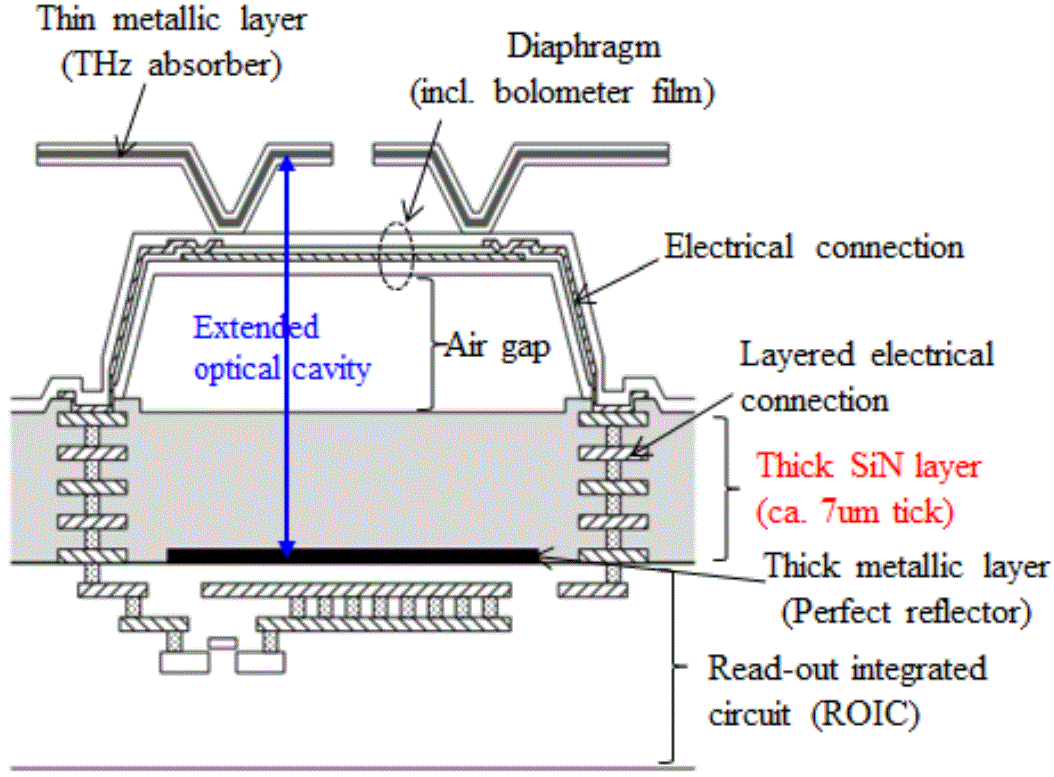
NEC Develops High Sensitivity Half-THz Image Sensor
NEC announces a new pixel structure for Thz array sensors and improved the Minimum Detectable Power per pixel (MDP) at 0.5 - 0.6 THz frequency by 10x over NEC's existing product. NEC currently produces and markets a THz camera IRV-T0831 equipped with a 320X240-pixel array sensor. However, NEC's latest pixel enables it to develop and produce a 640X480-pixel array sensor which has four times the number of pixels than the current model. NEC has also developed a camera equipped with the array sensor, making it one of the world's largest number of pixels at a THz frequency band.
"NEC has been addressing the development of a highly sensitive real-time uncooled terahertz camera and the improvement in the sensitivity of terahertz array sensors since the development of a highly sensitive bolometer-type uncooled two-dimensional terahertz array sensor in April 2008," said Dr. Naoki Oda, Executive Engineer, Radio Application, Guidance and Electro-Optics Division, NEC. "Going forward, NEC will pursue the development and production of terahertz imaging equipment using the present results and contribute to a variety of fields such as non-destructive inspection, medicine/drug development, and illegal object detection."
To improve the sensitivity, NEC expands the length of the optical cavity structure from 3 - 4 μm of the conventional value to 15 μm, which is formed between a thick metallic layer (perfect reflector) on a readout integrated circuit and thin metallic layer (THz absorber) on a pixel: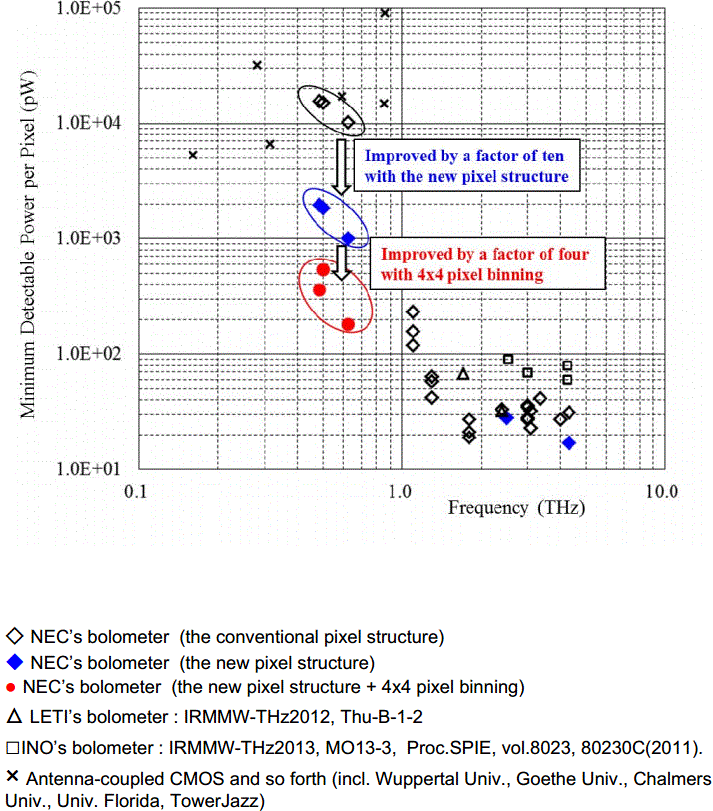
 |
| Conventional pixel used in the existing THz camera IR/V-T0831 |
 |
| New pixel structure with a thick SiN layer to extend optical cavity length |
Sony Announces Stacked Sensor with Phase AF Pixels
Sony announces the 21MP 1/2.4-inch Exmor RS IMX230 for smartphone cameras. It is said to be the industry's first CMOS sensor for smartphones to be equipped with an onboard image plane phase detection AF signal processing function supporting focus tracking of fast-moving subjects. Its HDR function now supports high-resolution still images and 4K video recording. The new CMOS image sensor will ship in April 2015.
Dedicated image plane phase detection AF pixels are used to calculate lens position and subject distance. Up to 192 AF points can be used. All calculations are instantaneously carried out by the stacked CMOS image sensor's internal image processing circuits:
HDR function works by setting two different exposures and applying the appropriate signal processing. Through improved pixel placement and signal processing, this new HDR imaging function is now compatible with both video recording and, by popular demand, still image capture, the latter a feature that was not available previously. (video HDR was first announced in 2012. When using the HDR movie function, the effective pixel count is reduced to 1/4 of its original number.) HDR function is also compatible with 4K video recording.


Dedicated image plane phase detection AF pixels are used to calculate lens position and subject distance. Up to 192 AF points can be used. All calculations are instantaneously carried out by the stacked CMOS image sensor's internal image processing circuits:
| Locations of 192 AF pixels |
HDR function works by setting two different exposures and applying the appropriate signal processing. Through improved pixel placement and signal processing, this new HDR imaging function is now compatible with both video recording and, by popular demand, still image capture, the latter a feature that was not available previously. (video HDR was first announced in 2012. When using the HDR movie function, the effective pixel count is reduced to 1/4 of its original number.) HDR function is also compatible with 4K video recording.
Sunday, November 16, 2014
Novatek Milestones
Novatek site confirms the internal image sensor design efforts and mentions a number of image sensor accomplishments over 2011-13 years:
All these sensors are not mentioned among the current products, and their status is unknown.
- Oct 2013:
Introduce Novatek's 1/4" VGA CMOS Sensor with CVBS output
Introduce Novatek's first 1/7" HD CMOS Sensor with MIPI Interface - Sep 2011:
Introduce Novatek's first HD CMOS sensor - Feb 2011:
Introduce Novatek's first CMOS sensor in 1.75um cell size technology
All these sensors are not mentioned among the current products, and their status is unknown.
Saturday, November 15, 2014
"Active Pixel Color Sampling" Story Goes On
SonyAlpha Rumors publishes more details on the allegedly oncoming Sony IMX189AEG "Active Pixel Color Sampling" sensor. The new material explains how the technology works. The RGB colored microlens layer is not rigidly attached to the sensor surface but rather is able slide along it. Each pixel has one sensing PD and three storage one that store the color info as the microlens layer slides:


A lot of data still looks illogical, such as over 9V saturation level, while the supply voltage is only 4.2V:


A lot of data still looks illogical, such as over 9V saturation level, while the supply voltage is only 4.2V:
Friday, November 14, 2014
Recent Nikon Patent Applications
Egami blog published a number of recent Nikon patent applications. One of them places small microlenses in corners between the big ones to reduce an optical crosstalk:


Another application, also quoted by New Camera site, proposes an HDR sensor with big and small pixels with big and small Bayer filter patterns:

Another application, also quoted by New Camera site, proposes an HDR sensor with big and small pixels with big and small Bayer filter patterns:
Himax Reports Q3 Results
Himax reports that its CMOS sensor sales improved significantly in Q3 2014: "Revenues from CMOS image sensors continued to show strength in the third quarter, increasing more than 20% from the previous quarter. Sales of the 2 and 5 megapixel products were particularly strong. However, the Company saw some delays in certain customers’ replacing older generation sensors with lower cost new designs which affected the Company’s gross margin. As expected, 8 megapixel CMOS image sensors began small volume sales in the third quarter and sales will accelerate in Q4 2014. The Company also launched its first 13 megapixel sensor during the fourth quarter. It anticipates 8 megapixel CMOS image sensors to continue to be the mainstream in 2015, and 13 megapixel the rising star in high end smartphones. This puts Himax firmly in the map as one of a handful of companies capable of offering a comprehensive product portfolio for main cameras of smartphones.
Additionally, the Company is also developing CMOS image sensors for non-consumer applications, for example, CMOS image sensor product line for automotive and surveillance applications, which typically enjoy higher margins and have less intensive competition. Collectively, the Company expects its CMOS image sensor business to more than double in 2014, making it a fast rising player in the market."
"...the Company continues to partner with various industry leading companies using its cutting edge and industry-dominant wafer level optics, or WLO, for the development of three technologies of the future, namely, array camera, special purpose sensors and microdisplay light guides for head-mounted devices. This product development often requires adoption of Himax’s internal CMOS image sensor, LCOS microdisplay and video processing algorithm teams. Himax sits in a leading and unique position as it is the only company in the industry which is able to offer such a one-stop total solution. To meet the anticipated demand growth for LCOS and WLO products, the Company is working on new plans to expand production capacity. The Company will report the progress in due course."
Thursday, November 13, 2014
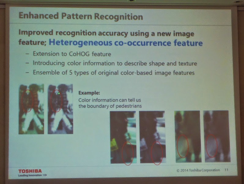
Toshiba Enhances Nighttime Performance of its ADAS Processor
Toshiba announces expansion of its line-up of image recognition processors for automotive applications with the launch of the TMPV760 series. Sample shipments of the first device, TMPV7608XBG will start in January 2015, with mass production scheduled for December 2016 onwards.
TMPV7608XBG features includes AEB (Autonomous Emergency Braking), TSR (Traffic Sign Recognition), LDW (Lane Departure Warning) and LKA (Lane Keeping Assist), HBA (High Beam Assistance), FCW (Forward Collision Warning), plus new applications that include TLR (Traffic Light Recognition) and AEB pedestrian (during both day and night), which will become part of the Euro NCAP testing program in 2018.
TMPV7608XBG integrates two Enhanced Co-occurrence Histograms of Oriented Gradients technology (CoHOG) accelerators for far higher accuracy image recognition at night. Connected to multiple, Full HD cameras, the processors analyzes color gradients in supplied images and achieves a night-time detection rate of pedestrians that matches the day-time recognition rate of the company’s current devices. TMPV7608XBG also supports a Structure from Motion (SfM) accelerator that realizes 3D reconstruction using the input stream of a monocular camera, and that can detect motionless obstacles on a road surface that are not detected by conventional pattern recognition.
Update: Nikkei Tech publishes few photos from Toshiba's presentation:


TMPV7608XBG features includes AEB (Autonomous Emergency Braking), TSR (Traffic Sign Recognition), LDW (Lane Departure Warning) and LKA (Lane Keeping Assist), HBA (High Beam Assistance), FCW (Forward Collision Warning), plus new applications that include TLR (Traffic Light Recognition) and AEB pedestrian (during both day and night), which will become part of the Euro NCAP testing program in 2018.
TMPV7608XBG integrates two Enhanced Co-occurrence Histograms of Oriented Gradients technology (CoHOG) accelerators for far higher accuracy image recognition at night. Connected to multiple, Full HD cameras, the processors analyzes color gradients in supplied images and achieves a night-time detection rate of pedestrians that matches the day-time recognition rate of the company’s current devices. TMPV7608XBG also supports a Structure from Motion (SfM) accelerator that realizes 3D reconstruction using the input stream of a monocular camera, and that can detect motionless obstacles on a road surface that are not detected by conventional pattern recognition.
 |
| TMPV760 applications |
Update: Nikkei Tech publishes few photos from Toshiba's presentation:
Wednesday, November 12, 2014
New Image Sensor Books
Recently, two image sensor books have been published. "High Performance Silicon Imaging: Fundamentals and Applications of CMOS and CCD sensors" is edited by Daniel Durini with contribution from many universities and well known imaging companies:

"Essential Principles of Image Sensors" by Takao Kuroda talks about essentials, just like its cover says:


"Essential Principles of Image Sensors" by Takao Kuroda talks about essentials, just like its cover says:

e2v Sensors Just Landed on Comet
e2v reports that five of its sensors are installed on ESA Rosetta space probe whose lander part has just landed on comet 67p/Churyumov-Gerasimenko - live updates are here. Rosetta was launched in 2004 and in August this year, achieved a milestone of becoming the first spacecraft to orbit a comet’s nucleus. Since then, Rosetta has been orbiting comet 67p and mapping its nucleus in great detail and in September, identified the potential landing site for its lander (Philae). The Philae has landed the comet today at 16:02 GMT.
e2v sensors involved in Rosetta mission:
On Rosetta:
On Philae:

e2v sensors involved in Rosetta mission:
On Rosetta:
- OSIRIS – the high resolution imaging camera. It has a narrow field and wide field camera.
- NAVCAM – the navigation camera.
- VIRTIS (Visible and Infrared Thermal Imaging Spectrometer) – which maps and studies the nature of the solids and the temperature on the surface of the comet. It also identifies gases, characterises the physical conditions of the comet and has helped to identify the best landing site (e2v’s devices are in the visible element of this instrument).
On Philae:
- ÇIVA (Comet nucleus Infrared and Visible Analyzer) – six identical micro-cameras take panoramic pictures of the surface of the comet. A spectrometer studies the composition, texture and albedo (reflectivity) of samples collected from the surface.
- ROLIS (Rosetta Lander Imaging System) – a CCD camera used to obtain high-resolution images during the descent of the lander and take stereo panoramic images of areas sampled by other instruments.
Tuesday, November 11, 2014
Selecting the Right Image Sensor
Point Grey publishes a video talk of its Director, Vladimir Tucakov, "Selecting The Right Camera Using EMVA 1288 Data, Vision 2014" with a popular explanation of image sensor metrics and their influence on a system performance:
Rumor: Sony to Introduce "Active Pixel Color Sampling" Technology
Chinese-language site cnBeta.com publishes what it says is a datasheet of Sony 1.5-inch 4.85MP IMX189AEG image sensor featuring "Active Pixel Color Sampling." The new stacked sensor features rectangular 9.78um x 4.89um pixels with global shutter. The site says that each pixel can sense three RGB colors. The sensor is planned to be used in an oncoming Sony Xperia Z4 smartphone. Very fast frame rates are quoted:

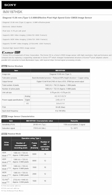
Another stacked Sony sensor appearing in other cnbeta.com post is 1MP IMX197HSK. It has a square 9.78um global shutter pixel and features high frame rates:
Via Android Headlines.

Another stacked Sony sensor appearing in other cnbeta.com post is 1MP IMX197HSK. It has a square 9.78um global shutter pixel and features high frame rates:

Via Android Headlines.
Monday, November 10, 2014
Rockchip to Enter Image Sensor Market?
International Conference on Optoelectronics and Microelectronics Technology and Application to be held on Nov. 12-14 in Tianjin, China, has an interesting paper by Qinghong Cao, Rockchip Electronics Co., China "A High Sensitivity CMOS Image Sensor Design with Complementary CFA and CCD Compatible Interface." Rockchip is one of the biggest application processors vendors in China, recently entered into a strategic alliance with Intel. The paper might be an early indication that the company is entering the image sensor market.
Update: It appears that Qinghong Cao, the author of the paper, used to work for Brigates, and possibly presents his former work on MCCD.
Update: It appears that Qinghong Cao, the author of the paper, used to work for Brigates, and possibly presents his former work on MCCD.
Sunday, November 09, 2014
Novatek Licenses CEVA Imaging and Vision DSP for Its Security SoCs
PR Newswire: CEVA announces that Novatek has selected the CEVA-MM3101 imaging and vision DSP for its next-generation SoC targeting the surveillance, action camera and automotive markets. Novatek will integrate the programmable CEVA-MM3101 into their SoC designs to add computer vision capabilities including scene analysis, machine vision, depth mapping and object detection in a flexible and power efficient manner.
"Integrating advanced vision processing capabilities with our imaging SoCs allows our customers to design products offering a new level of interactivity with the real world and show real product differentiation," Tommy Chen, VP at Novatek. "The CEVA-MM3101 imaging and vision DSP provides the processing horsepower while extending the device battery life and flexibility to implement innovative, intelligent imaging algorithms for any end application."
"We are pleased to partner with Novatek and excited by the potential offered by integrating our advanced imaging and vision DSP into their SoC roadmap," said Gideon Wertheizer, CEO of CEVA. "This is another instance of the growing popularity of the CEVA-MM3101 as a dedicated processor for computer vision and enables Novatek and their customers to reuse the design to address multiple market segments."
 |
| CEVA-MM3101 applications |
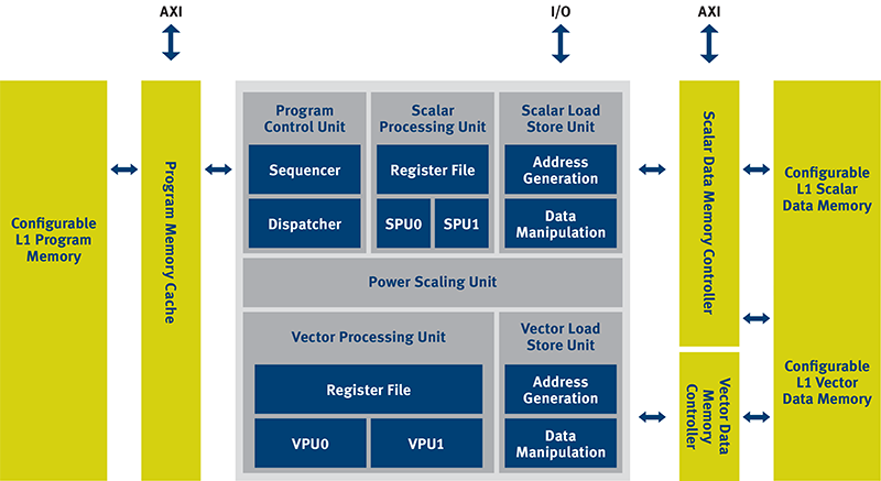 |
| CEVA-MM3101 architecture |
Saturday, November 08, 2014
Lytro Offers its Lightfield Photography Platform
Imaging Resource: Lytro announces Lytro Platform and Lytro Development Kit (LDK) opening a possibility to design a customized light field camera for any application.

 |
| LDK illustration. Actual may differ from the illustration. |
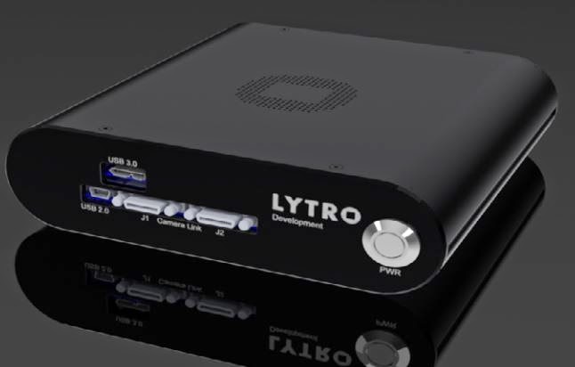 |
| LDK illustration. Actual may differ from the illustration. |
Friday, November 07, 2014
Is Mobile Future Square?
One of the recent mobile phone trends is a dual rear camera where the two cameras are 90-deg rotated with respect to each other to shoot pictures in horizontal and vertical direction, such as in Pixavi ImpactX phone:


Omnivision patent application US20140320715 "Imaging systems and methods using square image sensor for flexible image orientation" by Bahman Haji-khamneh, Harish Iyer, and Vinoo Margasahayam, implements this feature with a single square image sensor:


Omnivision patent application US20140320715 "Imaging systems and methods using square image sensor for flexible image orientation" by Bahman Haji-khamneh, Harish Iyer, and Vinoo Margasahayam, implements this feature with a single square image sensor:
Subscribe to:
Posts (Atom)