Sony announces that is has developed the world's first ghost catching device - Proton Pack equipped with a state-of-the-art, miniaturized superconducting synchrotron, which accelerates injected protons from a hydrogen plasma cell to capture ectoplasmic matter. The Proton Pack integrates the super slow motion video camera, allowing users to capture the matter in 960 fps rate and accurately record the movement of its target.
The company's official Youtube video explains the new product functionality:
Thursday, March 31, 2016
Wednesday, March 30, 2016
4-Base Color Vision in Humans
DNews posts a nice educational video talking about some people seeing life in 4 base colors, rather than in usual 3. Researchers claim that "Some 12% of women are carriers of the mild, X-linked forms of color vision deficiencies called “anomalous trichromacy.” Owing to random X chromosome inactivation, their retinae must contain four classes of cone rather than the normal three."
Pinnacle Licenses HDR IP Cores
PRWeb: Pinnacle Imaging Systems announces its Ultra HDR IP cores and HDR video capture technology, proven in its previous still-image software implementation. Ultra HDR provides adaptive tone mapping of HDR scenes up to 19 EV or 115 dB and can capture 120 fps (merging four exposures per frame), and stream full 1080 HDMI tone mapped video for display at up to 60 fps in real time.
“Even the most modern image sensors are limited in the dynamic range which they can capture,” said Alfred Zee, President & CEO of Pinnacle Imaging Systems. “We believe that cameras should be able to provide the same contrast range that we naturally see with our own eyes, so we based our technology on the human vision model. It’s this unique approach that allows our Ultra HDR technology to deliver such color-accurate, high contrast video quality.”
Pinnacle Ultra HDR technology addresses many of the complexities involved in HDR video capture including:

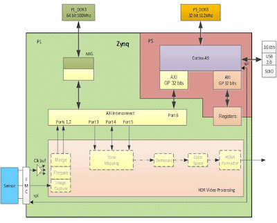
FPGA-based Ultra HDR Dev. Platform resource requirements:
Existing FPGA Based Platform (full video path)
“Even the most modern image sensors are limited in the dynamic range which they can capture,” said Alfred Zee, President & CEO of Pinnacle Imaging Systems. “We believe that cameras should be able to provide the same contrast range that we naturally see with our own eyes, so we based our technology on the human vision model. It’s this unique approach that allows our Ultra HDR technology to deliver such color-accurate, high contrast video quality.”
Pinnacle Ultra HDR technology addresses many of the complexities involved in HDR video capture including:
- Automatic Ghost Removal & Halo Reduction – Compensates for movement between HDR exposures, from minimal camera motion to moving objects between frames
- Adaptive Local Tone Mapping – Automatically optimizes the tone mapping parameters based on the shadow and highlight areas of each individual video frame
- Automatic White Balance Controls – Automatically calculates proper white balance settings for any scene or lighting condition
- Automatic Exposure Controls – Real time calculation and adjustment of the sensor’s exposure settings based on an automatic or manually selected region of interest to allow accurate exposure throughout a scene
- Shadow Exposure Bias Option – Ability to bias tone mapping with an additional Shadow Tracking option during the Auto Exposure mode for optimal shadow detail and data preservation, a key requirement for surveillance applications


FPGA-based Ultra HDR Dev. Platform resource requirements:
Existing FPGA Based Platform (full video path)
- 40k slices, 308 DSP blocks
- 600k byte internal RAM (155 36k bit BRAM, 32 18k bit BRAM)
- 28G bit external DDR3 BW, memory for frame buffers
- Currently running at 148.5MHz clock rate
- Can be ported to low cost Altera (Cyclone) or Xilinx (Artix)
- Single input data stream, one frame/exposure at a time.
- IP size is 480k gates coupled with 59k bytes of RAM.
- Requires 19G bit/s bandwidth on an external DDR port for frame buffering.
- IP size is 327k gates coupled with 300k bytes of RAM.
- Requires 9.5G bit/s bandwidth on an external DDR port for frame buffering.
Tuesday, March 29, 2016
ResearchInChina on ADAS Transition to Stereo Cameras
ResearchInChina's "Global and China Vision ADAS Industry Report, 2015-2020" report forecasts that ADAS systems will adapt stereo cameras and abandon mono ones:
"Camera-based vision ADAS systems can be divided into several categories of applications: 1) Lane Detection, i.e., LDW/LKA/LCA (Lane Centering Assist) to prevent the car from deviating in the working state of either ACC or TJA (Traffic Jam Assist); 2) Obstacles Detection and Recognition, i.e., FCW (Forward Collision Warning)/AEB (Autonomous Emergency Braking); 3) Surroundings Display, i.e., Parking Assist, including Rear View and 360°Surround View. 4) BSD (Blind Spot Detection); 5) HBA (High Beam Assist) and Night Vision.
In application field, warning-only ADASs will gradually exit market, while the ADASs with actuator represent the mainstream in the future. For example, it is hard for drivers to take prompt countermeasures, as the warning time of FCW is no more than 3 seconds. Moreover, AEB (Autonomous Emergency Braking) may become the most important ADAS application. AEB will be a mandatory safety function across the world during 2021-2025.
Future orientation of development will be stereo camera rather than mono camera, especially in AEB field. As AEB concerns human life, there must be as much performance redundancy as possible, thus ensuring the safety of drivers to the utmost extent. Stereo camera has an overwhelming advantage over mono camera in the aspect of pedestrians recognition. However, the majority of companies (OEMs & Tier 1 suppliers) still adopt mono camera, as AEB is largely an optional component rather than a standard one, and the costs of stereo camera are much higher, resulting in higher price and low popularity.
Pedestrians Recognition will be a must of next-generation AEB, meaning that stereo camera has to be employed. Mercedes-Benz, Subrau, Jaguar, and Suzuki have adopted stereo camera from the very beginning, while VW, Toyota, Honda, and Nissan all employ stereo camera in their experimental models. As to Tier 1, Hitachi Automotive System has used stereo camera at the very start, while Continental, Bosch, Denso, and Fujitsu Ten see stereo camera as the priority of development. These companies are iconic ones in automobile industry and their moves represent the direction of automobile industry as a whole.
Global automotive camera module shipments approximated 50.3 million pieces in 2015 and are expected to reach 62.1 million pieces in 2016, 141 million pieces in 2020, and 246 million pieces in 2025. There are three cameras on each light vehicle on average, respectively for LKA, AEB, and Parking. Unlike mobile phone camera modules, automotive camera modules are highly demanding on reliability and range of operating temperature. Major vendors are Panasonic, Sony, Valeo, Fujitsu Ten, MCNEX, Magna, Gentex, Continental, and Hitachi. Panasonic ranks first globally in terms of market share and is far ahead of the second place.
Global automotive vision system market size was worth about USD3.1 billion in 2015 and is expected to hit USD6.1 billion in 2020. Magna, TRW (ZF), Hitachi Automotive System, and Continental are in the first camp, with Magna being the world’s largest, and Autoliv, Valeo, Denso, Fujitsu-ten, and Bosch are in the second camp. As the demand from carmakers varies greatly, the market concentration has been lower and this will continue for a considerable time."
Hamamatsu Publishes Camera Simulator
Hamamatsu publishes a camera simulator showing an expected camera output for various image sensor and camera setups. Unfortunately, many image sensor imperfections are omitted, such as all color effects, hot and bad pixels, lens shading, RTN, PRNU, etc. Still a nice simulator, though:


Rumor: Sony Low Cost Security Sensor for Less than $3
Sony low cost STARVIS sensor, IMX323, for security and surveillance applications is reportedly offered for less than $3 in volume in China. The 1080p30 1/2.9-inch sensor is based on 2.8um pixels. A complete datasheet of the new sensor can be downloaded here.


Monday, March 28, 2016
BSI CMOS Sensor Market Reasearch
P&S Market Research publishes "Global Industry Insight: BSI CMOS Image Sensor Market Size, Share, Development, Growth and Demand Forecast to 2020." Few insights from the report:
"North America leads the backside illumination (BSI), complementary metal oxide semiconductor (CMOS) image sensor market, due to several design and technological improvements in this technology... The Asia-Pacific BSI CMOS image sensor market is expected to grow at the highest rate, in the coming years, due to which, it is expected to become the largest market, in the coming years. One of the key reasons for high growth of Asia Pacific in this market is its swift transition from analog to digital systems...
BSI CMOS image sensors eliminate the bulk substrate in the devices to decrease diffusion component of dark current and electrical crosstalk. BSI CMOS image sensors have higher quantum efficiency, which in turn enhances the production of output images with similar signal to noise ratio (SNR). However BSI CMOS image sensors are mechanically weaker, due to wafer thinning, which results in more chances of breakage for a large BSI CMOS image sensor."
Friday, March 25, 2016
InVisage vs InvenSense
EETimes publishes an article "What Do InVisage & InvenSense Have in Common?" by Peter Clarke, comparing Invisage and Invensense business models. While Invensense is successful at MEMS inertial sensors market, licensing its process to others does not bring much income for the company. So, the article questions whether this approach can work for Invisage.
On Chip CMOS Vision Systems for High-Speed Applications Thesis
Seville University, Spain publishes "On Chip CMOS Vision Systems for High-Speed Applications" PhD Thesis by Francisco Jose Jimenez Garrido, dated by Oct. 2015 and devoted to smart sensors with fast in-pixel processing:


Thursday, March 24, 2016
Brookman Announces 33MP 120fps Super35mm UHDTV Sensor
Brookman Technology delivers engineering samples of 33MP, 120fps BT3300N for 8K Super Hi-Vision broadcast, which was co-developed with NHK and Prof. Kawahito's Group of Shizuoka University. BT3300N is said to be the only image sensor (as of January 2016) that meets the full specifications of the Super Hi-Vision (8K, 120fps) and its optical format is Super 35mm. The new sensor is based on 3.2um pixels and features 14b 2-stage ADC.
8K Super Hi-Vision is set to begin test broadcasting in 2016 and roll out full broadcasting by 2018.
MarketWired: Silvaco announces that Brookman has adopted Silvaco's power integrity tool suite InVar Power-IR-Thermal for the design and development of its CMOS sensor products. InVar Power analyzes dynamic power consumption; InVar IR analyzes voltage drops in power sources and signal networks; and InVar Thermal performs thermal analysis at the full chip level. Concurrent observations of power, IR and thermal make it possible to perform real-time analysis, considering the effect of heat generation.
Brookman Technology's President, Satoshi Aoyama, stated, "8K standard demands the challenging specs to sensors, which are 33Mega-pixel resolution, 120 frames/second speed and 12-bit image gradation. This large and high-speed sensor is facing the issue of voltage drops so critically that the analysis by InVar IR is extremely helpful. In addition, as for the problem regarding the degradation of image due to intra-chip heat generation, we expect that InVar Thermal contributes effectively to the shortening of development TAT, as well as the improvement of design quality."
8K Super Hi-Vision is set to begin test broadcasting in 2016 and roll out full broadcasting by 2018.
 |
| Brookman BT3300N |
MarketWired: Silvaco announces that Brookman has adopted Silvaco's power integrity tool suite InVar Power-IR-Thermal for the design and development of its CMOS sensor products. InVar Power analyzes dynamic power consumption; InVar IR analyzes voltage drops in power sources and signal networks; and InVar Thermal performs thermal analysis at the full chip level. Concurrent observations of power, IR and thermal make it possible to perform real-time analysis, considering the effect of heat generation.
Brookman Technology's President, Satoshi Aoyama, stated, "8K standard demands the challenging specs to sensors, which are 33Mega-pixel resolution, 120 frames/second speed and 12-bit image gradation. This large and high-speed sensor is facing the issue of voltage drops so critically that the analysis by InVar IR is extremely helpful. In addition, as for the problem regarding the degradation of image due to intra-chip heat generation, we expect that InVar Thermal contributes effectively to the shortening of development TAT, as well as the improvement of design quality."
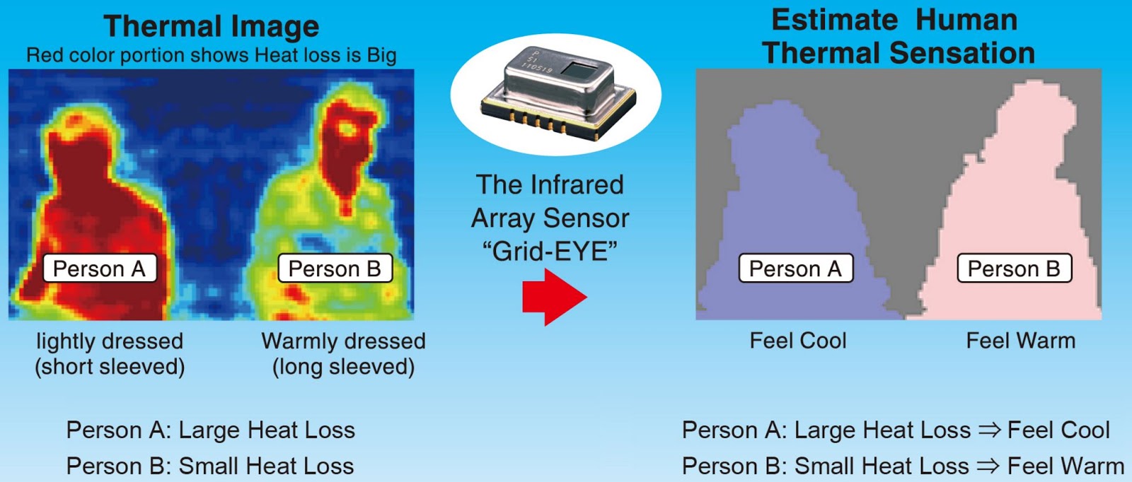
Panasonic Thermal Sensing Solution
BusinessWire: Panasonic develops a thermal sensation estimation method using its infrared array sensor Grid-EYE. The thermal sensation estimation method recognizes the human sensations of hot and cold by calculating heat loss based on the difference between human surface temperature and ambient temperature. The thermal sensing solutions Panasonic provides are a super-resolution algorithm using Grid-EYE, an infrared array sensor, to measure the temperature distribution in detail and detect objects, thereby achieving air conditioning suitable for sensed temperature by combining the obtained data and thermal sensation estimation method.

The 2014 company video explains Grid-Eye imager features:
The 2014 company video explains Grid-Eye imager features:
Wednesday, March 23, 2016
VLSI Symposia Accepted Papers
VLSI Circuit and Technology Symposia to be held on June 13-17, 2016 in Honolulu, HI, publishes accepted paper list, with quite a few image sensor papers:
“Accelerating the Sensing World through Imaging Evolution”, Tetsuo Nomoto, VP and SGM, SONY
The evolution of CMOS Image Sensors (CIS) and the future prospect of a “sensing” world utilizing advanced imaging technologies promise to improve our quality of life by sensing anything, anywhere, anytime. Charge Coupled Device image sensors replaced video camera tubes, allowing the introduction of compact video cameras as consumer products. CIS now dominates the market for digital still cameras created by its predecessor and, with the advent of column-parallel ADCs and back-illuminated technologies, outperforms them. CIS’s achieve better signal to noise ratio, lower power consumption, and higher frame rate. Stacked CIS’s continue to enhance functionality and user experience in mobile devices, a market that currently comprises over one billion new image sensors per year. CIS imaging technologies promise to accelerate the progress of sensing world by continuously improving image quality, extending detectable wavelengths, and further improving depth resolution and temporal resolution.
- A 220pJ/Pixel/Frame CMOS Image Sensor with Partial Settling Readout Architecture, Ji, Stanford University
- An 8.3M‐pixel 480fps Global‐Shutter CMOS Image Sensor with Gain‐Adaptive Column ADCs and 2‐on‐1 Stacked Device Structure, Oike, Sony
- A Dead‐time Free Global Shutter CMOS Image Sensor with in‐pixel LOFIC and ADC using Pixel‐wise Direct Connections, Sugo, Tohoku Univ.
- White Spots Reduction by Ultimate Proximity Metal Gettering at Carbon Complexes Formed underneath Contact Area in CMOS Image Sensors, Yamaguchi, Renesas Electronics Corporation
- Enabling monolithic 3D image sensor using large-area monolayer transition metal dichalcogenide and logic/memory hybrid 3D+IC, Yang, National Nano Device Laboratories
- Back‐illuminated voltage‐domain global shutter CMOS image sensor with 3.75µm pixels and dual in‐pixel storage nodes, Stark, University of Edinburgh, UK
- Broadband THz Spectroscopic Imaging based on Fully Integrated 4×2 Digital‐to‐Impulse Radiating Array with Full‐Spectrum of 0.03‐1.03THz in Silicon, Assefzadeh, Rice University
- Novel Pixel Structure with Stacked Deep Photodiode to Achieve High NIR Sensitivity and High MTF, Takahashi Hiroki, TowerJazz
“Accelerating the Sensing World through Imaging Evolution”, Tetsuo Nomoto, VP and SGM, SONY
The evolution of CMOS Image Sensors (CIS) and the future prospect of a “sensing” world utilizing advanced imaging technologies promise to improve our quality of life by sensing anything, anywhere, anytime. Charge Coupled Device image sensors replaced video camera tubes, allowing the introduction of compact video cameras as consumer products. CIS now dominates the market for digital still cameras created by its predecessor and, with the advent of column-parallel ADCs and back-illuminated technologies, outperforms them. CIS’s achieve better signal to noise ratio, lower power consumption, and higher frame rate. Stacked CIS’s continue to enhance functionality and user experience in mobile devices, a market that currently comprises over one billion new image sensors per year. CIS imaging technologies promise to accelerate the progress of sensing world by continuously improving image quality, extending detectable wavelengths, and further improving depth resolution and temporal resolution.
Tuesday, March 22, 2016
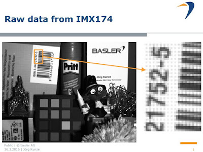
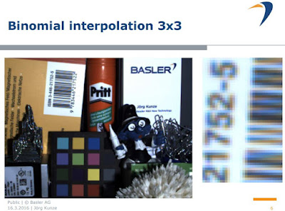
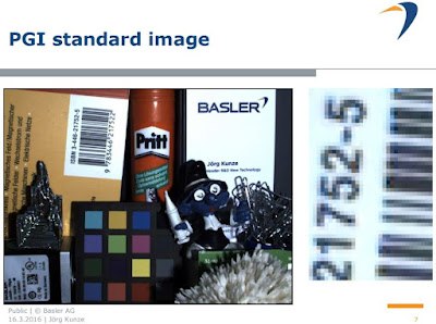
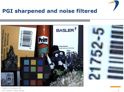
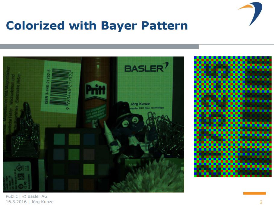
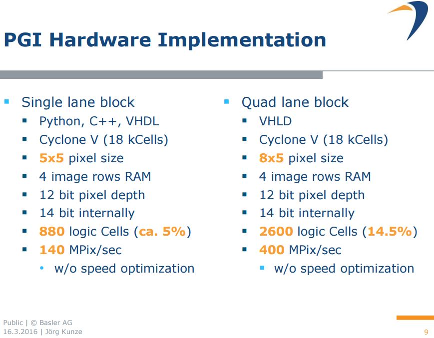
Basler Improves on Demosaicing Algorithms
Jörg Kunze from Basler AG kindly allowed me to publish few slides from his presentation at the London Image Sensors 2016 conference about his novel Debayering algorithm called PGI.
His implementation is a hardware-efficient single-step 5x5 pixel algorithm, which performs a zipper-free high-quality Bayer-pattern interpolation up to the theoretical frequency limit, color-anti-aliasing, sharpness enhancement and noise reduction together. The pictures look very convincing. Basler has currently a single-lane FPGA implementation with a throughput of 140 MPix/s using 880 Cyclone V logic cells and a quad lane implementation with a throughput of 400 MPix/s using 2600 logic cells. Jörg says, Basler is interested in licensing, cross-licensing or technology exchange.


His implementation is a hardware-efficient single-step 5x5 pixel algorithm, which performs a zipper-free high-quality Bayer-pattern interpolation up to the theoretical frequency limit, color-anti-aliasing, sharpness enhancement and noise reduction together. The pictures look very convincing. Basler has currently a single-lane FPGA implementation with a throughput of 140 MPix/s using 880 Cyclone V logic cells and a quad lane implementation with a throughput of 400 MPix/s using 2600 logic cells. Jörg says, Basler is interested in licensing, cross-licensing or technology exchange.


Monday, March 21, 2016
Honda to Release Autonomous Driving Civic
WSJ: Honda is releasing automated highway driving features on its entry-level vehicle Civic LX sedan. With price tag of $20,440 it makes it accessible to significantly more buyers, including younger ones.
As auto makers offer the components needed to power these functions in option packages as low as $1,800, they are being snapped up at a far higher rate than electrified vehicles.
Via Videantis news.
As auto makers offer the components needed to power these functions in option packages as low as $1,800, they are being snapped up at a far higher rate than electrified vehicles.
Via Videantis news.
Mediatek Launches Imagiq ISP
MediaTek announces the Imagiq ISP foir Helio high-end smartphone chipset solution.
As dual cameras are becoming standard on high-end smartphones, MediaTek Imagiq offer features enhancing the dual photography:

As dual cameras are becoming standard on high-end smartphones, MediaTek Imagiq offer features enhancing the dual photography:
- Real-Time Large Aperture Depth-of-Field Effect – With the built-in 3D sensor, the ISP can capture depth mapping in real-time, and with a large aperture of greater than f/0.8, it can produce large aperture depth-of-field effects in real-time even for previews.
- Reality Depth of Field (DOF) – Users can map objects and backgrounds to multiple layers with a DOF feature. The smartphone can smartly position the object and background and apply creative effects to each layer in real time to produce photos or videos with DOF effects.
- Bayer and Mono Cameras – This multiple-sensor design can capture three times the light of a traditional single-bayer sensor, thus reducing image noise and increasing quality.
- Dual Camera Zoom – The ISP is equipped with a wide-angle lens and a telescope in its dual camera system. Imagiq combines these wide-angle and zoomed captured images into one image.
- Hybrid Autofocus (PDAF and Laser Auto Focus) – Combining PDAF and Laser AF to realize a faster autofocus speed, which is also applicable in dimly lit environments.
- Pixel-Level Auto Focus – A focus speed is four times that of traditional autofocus, making it especially suitable for shooting fast-moving objects in real-time.
- New De-Mosaic and Sharpness Engine – With its large-scale texture recognition and implementation of adaptive color image abilities, Imagiq produces smoother and sharper images when taking photos in dimly lit environments.
- New Adaptive De-Noising Engine – Imagiq reduces image noise even in low-light environments
- Automatic Image Stabilization (AIS) – Imagiq can rapidly combine four consecutively captured images into one image, eliminating blur effects from camera shake.
- TrueBright Engine – With first-time RWWB sensor support, Imagiq powers twice the sensitivity to light of a traditional RGB sensor.
- EIS and Gyro – Using a hardware engine to predict motion, Imagiq eliminates a video’s camera shake and distortion.
- 1/32 Super-Slow Motion – In addition to supporting 720p video, Imagiq can shoot 1080p video at 480 fps in 1/32 super-slow motion playback, resulting in a 960 FPS video. Users are also able to edit videos using super-slow motion.
- Temporal Noise Reduction – Imagiq uses temporal noise reduction to locate and reduce pixel movement in videos, resulting in cleaner and more detailed video quality in both video previews and filming.
- 4K HDR Shooting – Support 4K HDR video shooting for the first time.


Sunday, March 20, 2016
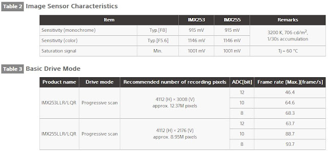
Sony Presents 9MP and 12.4MP Global Shutter Sensors
Sony 3.45um global shutter pixel, said to be the smallest in the industry, is the base of two new sensors: IMX253LLR/LQR 1.1-inch 12.37MP and IMX255LLR/LQR 1-inch 8.95MP, available in both monochrome (LLR) and color (LQR) versions.
The company's Youtube video shows global shutter advantages:
The company's Youtube video shows global shutter advantages:
Saturday, March 19, 2016
Blackmagic Cancels Global Shutter Mode on its Newest Cameras
Blackmagic Design CEO, Grant Petty, posted an update on the global shutter problems in its newest cameras URSA Mini 4.6K and the Micro Cinema Camera, originally expected to ship in Oct. 2015, but delayed up to now:
"We have really appreciated everyone’s patience in waiting for these cameras and apologize for the delay. It took much longer than we had thought to get the cameras to where we needed them to be, but I am incredibly proud to bring 15 stop, Super 35 true digital film cameras to everyone...
However the big reason for the delay is the problems we were having with the global shutter feature in both of these cameras. The problems are different between the models and on the Micro Cinema Camera we have been seeing random bad pixels when in global shutter mode. On the URSA Mini 4.6K we have been seeing problems with sensor calibration when using global shutter.
Our engineers have been killing themselves working on this for months, but the performance is just not where it needs to be for us to feel comfortable shipping with global shutter, and so we have had to remove the global shutter feature from both these cameras to allow them to ship.
Obviously this is very upsetting for us, as we really wanted to produce high dynamic range cameras that also had a global shutter for an all in one design. The reality is that this is just one feature on cameras that are ready right now to shoot with and get incredible results. So we have made the decision to ship now."
Thanks to TG for the info!
"We have really appreciated everyone’s patience in waiting for these cameras and apologize for the delay. It took much longer than we had thought to get the cameras to where we needed them to be, but I am incredibly proud to bring 15 stop, Super 35 true digital film cameras to everyone...
However the big reason for the delay is the problems we were having with the global shutter feature in both of these cameras. The problems are different between the models and on the Micro Cinema Camera we have been seeing random bad pixels when in global shutter mode. On the URSA Mini 4.6K we have been seeing problems with sensor calibration when using global shutter.
Our engineers have been killing themselves working on this for months, but the performance is just not where it needs to be for us to feel comfortable shipping with global shutter, and so we have had to remove the global shutter feature from both these cameras to allow them to ship.
Obviously this is very upsetting for us, as we really wanted to produce high dynamic range cameras that also had a global shutter for an all in one design. The reality is that this is just one feature on cameras that are ready right now to shoot with and get incredible results. So we have made the decision to ship now."
 |
| The Micro Cinema Camera |
 |
| Image sensor area magnified |
Thanks to TG for the info!
Thursday, March 17, 2016
Analog Devices Acquires Swiss Image Sensor Company
EETimes-Europe: Analog Devices Inc. has acquired Snap Sensor SA (Neuchatel, Switzerland), a maker of HDR and other specialized image sensors, for an undisclosed some of money.
Snap Sensor was founded in 2011 as a spin-off from an 8-year research program at Swiss research and technology organization CSEM. "SNAP Sensor’s cutting-edge optical technology and vision software and algorithm expertise allow us to continue unlocking new possibilities for our customers in a wide range of IoT applications such as building automation, building security, city management, transportation, and more,” said Michael Murray, GM of Industrial Sensing, Analog Devices. “This acquisition further enhances our sensing portfolio and ensures that we’re helping customers realize the best possible outcomes from IoT solutions.”
The SNAP Sensor team will remain in Switzerland to establish a new Analog Devices R&D center and continue its close collaboration with CSEM. The acquisition will enhance Analog Devices’ Blackfin Low Power Imaging Platform (BLiP). “Our team is very enthusiastic about joining Analog Devices,” said Pascal Dorster, CEO of SNAP Sensor. “This provides us access to the engineering, supply-chain, and commercialization resources needed to accelerate our growth and continue advancing our technology vision.”


Caterpillar Self-Driving Trucks
AutoSens Conference to be held on Sept. 20-22, 2016 in Brussels, Belgium, publishes an interview with Bibhrajit Halder, a Software Technical Specialist in the ADAS and Self-Driving team, Faraday Future automotive startup. The interview touches Caterpillar work on self-driving vision-based mining trucks:
 |
| Caterpillar self-driving track weights 390 tonnes (860,000 lb) fully loaded |
Wednesday, March 16, 2016
31st ICHSIP
The 31st International Congress on High Speed Imaging and Photonics (ICHIP) will be held in Osaka, Japan on Nov. 7-10, 2016. So far, the list of 20 invited speakers has been announced, most of them showing previews of their work:
Liang Gao (University of Illinois, USA)
Compressed Ultrafast Photography: Catching photons on the fly by Compressed Ultrafast Photography
Keisuke GODA (University of Tokyo)
Sub-picosecond Imaging of “Propagating Phonons”
and many more on the Congress web site.
Thanks to RT for the link!
Liang Gao (University of Illinois, USA)
Compressed Ultrafast Photography: Catching photons on the fly by Compressed Ultrafast Photography

Keisuke GODA (University of Tokyo)
Sub-picosecond Imaging of “Propagating Phonons”

and many more on the Congress web site.
Thanks to RT for the link!
Movidius and DJI Bring Vision-Based Technology to DJI Phantom 4
MarketWired: Movidius and DJI announce that Movidius Myriad 2 vision processor is used in DJI’s flagship Phantom 4 aircraft, giving it the ability to sense and avoid obstacles in real time and hover in a fixed position without the need for a GPS signal.
The agreement is said to mark an industry first in making advanced visual guidance systems a standard feature for consumer drones.
“Movidius’ vision processor platform, Myriad 2, met the rigorous requirements we set for our flagship product, and we look forward to continued collaboration with Movidius as we push the boundaries in the drone market,” said Paul Pan, Senior Product Manager at DJI.
“DJI has set the direction for the future of the drone market and we are excited to incorporate Movidius’ low power artificial vision intelligence technology into DJI drones moving forward,” said Sean Mitchell, COO of Movidius. “Moving the technology from a demonstration to a highly reliable production worthy stage was a tremendous effort for both DJI and Movidius. The DJI Phantom 4 launch represents a milestone for the future of visually aware devices. We believe we are entering the golden age of embedded computer vision and our technology has placed Movidius at the forefront of this trend.”
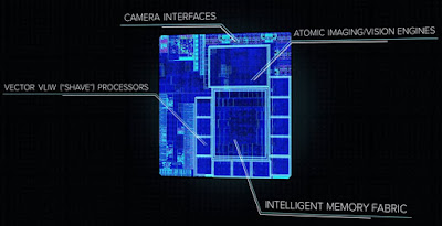
Movidius publishes a Youtube video explaining Phantom 4 vision features:
The agreement is said to mark an industry first in making advanced visual guidance systems a standard feature for consumer drones.
“Movidius’ vision processor platform, Myriad 2, met the rigorous requirements we set for our flagship product, and we look forward to continued collaboration with Movidius as we push the boundaries in the drone market,” said Paul Pan, Senior Product Manager at DJI.
“DJI has set the direction for the future of the drone market and we are excited to incorporate Movidius’ low power artificial vision intelligence technology into DJI drones moving forward,” said Sean Mitchell, COO of Movidius. “Moving the technology from a demonstration to a highly reliable production worthy stage was a tremendous effort for both DJI and Movidius. The DJI Phantom 4 launch represents a milestone for the future of visually aware devices. We believe we are entering the golden age of embedded computer vision and our technology has placed Movidius at the forefront of this trend.”


Movidius publishes a Youtube video explaining Phantom 4 vision features:
Tuesday, March 15, 2016
Caeleste & SPIE Workshop
Caeleste presents "The future of high-end imaging" workshop to be held on Wednesday, April 6, 2016 from 13:30 – 17:40 at the Square meeting Center, Kunstberg – Mont des Arts in Brussels. This seminar will run in conjunction with the SPIE Photonics Europe Conference.
Caeleste brought together experts in the field and they provide their view on the trends in future high-end image sensors:
Caeleste brought together experts in the field and they provide their view on the trends in future high-end image sensors:
- Jan Bosiers, Teledyne-Dalsa: Wafer-scale CMOS imagers for medical X-ray imaging
- Benoit Dupont – Pyxalis: 20 bit image sensors using dual processor architectures
- Gert Finger, ESO: Large format, high speed sub-electron noise image sensors for ground-based astronomy
- Jochem Hermann, Adimec: CCD is history, CMOS is the future: ‘Still many challenges ahead!’
- Ajit Kumar Kalgi, Caeleste: High Dynamic Range, shot noise limited Image sensors with global shutter.
- Nick Nelms, ESA-ESTEC: High-performance image sensors in space – the shape of things to come.
- Karsten Sengebusch, Eureca: Prediction of the performance and image quality of CMOS image sensors.
Monday, March 14, 2016
EETimes Interviews Invisage CEO
EETimes-Europe publishes an interview with Jess Lee, Invisage CEO. Few quotes:
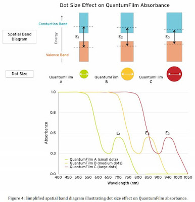
"We have not said to much about the material structure of QuantumFilm. There are concerns over cadmium in quantum dots so the first thing to say is there is no cadmium. What we have said is that it is a metal-chalcogenide material, similar to a II-VI material surrounded by ligands in a matrix.
The dots are of a diameter of between about 3-micron and 5-micron and it is these dimensions that affect the electron band structure and govern the sensitivity to light.
We are limited by the state of silicon I/O and analog-to-digital converters. As that rises we can go at hundreds, even thousands of frames per second. There is no difference between us and comparable CMOS image sensors.
We see QuantumFilm as a platform used by us as the first and second customer. To have third and fourth customers is better for us. We are prepared to work with partners to enable them, with QuantumFilm. We wouldn't license the technology out but there are a number of other ways to enable partners.
...we are on a mature silicon platform – 110nm. It's a very different capital investment process there. We have our own fab in Taiwan but it is only focused on a couple of processes – a spin-on process to add the film and the definition of the pixels."
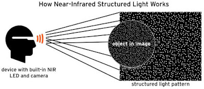
Invisage white paper linked on the last page of the article discusses NIR imaging applications:

"We have not said to much about the material structure of QuantumFilm. There are concerns over cadmium in quantum dots so the first thing to say is there is no cadmium. What we have said is that it is a metal-chalcogenide material, similar to a II-VI material surrounded by ligands in a matrix.
The dots are of a diameter of between about 3-micron and 5-micron and it is these dimensions that affect the electron band structure and govern the sensitivity to light.
We are limited by the state of silicon I/O and analog-to-digital converters. As that rises we can go at hundreds, even thousands of frames per second. There is no difference between us and comparable CMOS image sensors.
We see QuantumFilm as a platform used by us as the first and second customer. To have third and fourth customers is better for us. We are prepared to work with partners to enable them, with QuantumFilm. We wouldn't license the technology out but there are a number of other ways to enable partners.
...we are on a mature silicon platform – 110nm. It's a very different capital investment process there. We have our own fab in Taiwan but it is only focused on a couple of processes – a spin-on process to add the film and the definition of the pixels."
Invisage white paper linked on the last page of the article discusses NIR imaging applications:


 |
| SparkP2 product overview |
PIDA on CMOS Sensor Market
CTimes quotes Photonics Technology & Industry Development Association (PIDA) saying that "in 2014 the total global CMOS sensor shipments amounted to 4.65 billion units. Chinese manufacturer Galaxycore was the top company, accounting for 21% of the shipments; whereas Japan’s Sony and the United States’ Omnivision made the second highest number of shipments at 19%. Meanwhile, low pixel VGA products showed the most rapid growth during the past few years.
Chinese cell phone manufacturers are winning over CMOS sensors that were manufactured by Sony, which has resulted in Sony’s proposed early expansion of investment."
Chinese cell phone manufacturers are winning over CMOS sensors that were manufactured by Sony, which has resulted in Sony’s proposed early expansion of investment."
Sunday, March 13, 2016
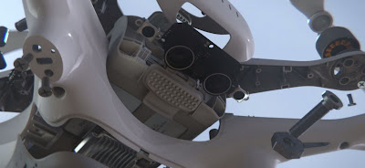
DJI Phantom 4 Drone Features 5 Cameras
Drones quickly become a sizable camera market. The latest DJI Phantom 4 drone has 5 cameras (1 for remote viewing and recording plus 4 for vision processing: follow me, depth , object recognition and tracking, visual navigation). DJI is the world's largest drone manufacturer, based in Shenzhen, China.
Thanks to FS for the info!
Thanks to FS for the info!
PDAF Pixel Report Update
Albert Theuwissen has updated his PDAF pixel characterization report with additional measurements focused on :
The Harvest Imaging site look is also updated and is much nicer now.
- the influence of the exposure time on the PDAF pixel signals and the possibility to extract useful focusing information from it,
- angular light dependency of the PDAF pixels.
The Harvest Imaging site look is also updated and is much nicer now.
Saturday, March 12, 2016
EMCCD Low Light Surveillance by ON Semi
EE Journal publishes ON Semi Michael DeLuca Youtube interview on EMCCD low light imaging for surveillance:
Samsung S5K2L1 ISOCELL vs Sony IMX260 Comparison
Phonearena quotes Finnish-language Taskumuro site making an unscientific comparison of Samsung Galaxy S7 equipped with Sony IMX260 and Samsung S5K2L1 dual-pixel AF sensors. One can judge the differences on real-life subjects with HDR mode off (many more pictures on the original site):


More PhoneArena thoughts on the comparison is here.


 |
| Sony sensor, click & download for full resolution |
 |
| Samsung sensor, click & download for full resolution |
More PhoneArena thoughts on the comparison is here.
Friday, March 11, 2016
MEMS Drive and OPPO Joint PR
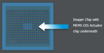
PRWeb: MEMS Drive and OPPO come up with a joint press release on their MEMS-based SmartSensor, the first image sensor-based image stabilizer for smartphones, also said to be the industry’s first sub-pixel-level optical image stabilizer.
While VCM smartphone cameras are limited to shake compensation on just two axes of movement, the new MEMS-based approach compensates for motion on three axes. This additional degree of mobility is said to vastly outperform traditional OIS technologies for smartphones, because it is faster – compensating for vibrations in 15 ms compared to 50 ms for lens-based technologies – and more accurate, and it allows for significantly lower power consumption.
MEMS Drive was founded to develop and advance the field of MEMS OIS technology for smartphone cameras. “The collaboration with OPPO has been very successful. The fact that OPPO is taking such an active role in co-developing this technology with MEMS Drive is accelerating our roadmap, and will ultimately come to benefit smartphone users sooner,” said Colin Kwan, CEO and founder of MEMS Drive.
“OPPO recognized that the MEMS Drive OIS actuator could vastly improve the end users’ camera experience. We therefore decided to invest in MEMS Drive and to co-develop the SmartSensor image stabilizer, and bring yet another significant advance in smartphone technology to market,” said King Liu, VP of Product Development at OPPO.
The advantages of MEMS Drive OIS are:
- 3 Axis stabilization: pitch, yaw and roll
- Fast (MEMS advantage)
- Low power consumption
- High precision
- Built-in 2 Axis accelerometer
- Compatible with any existing AF, shutter and Zoom actuators
- 3D capture
- Super resolution


Thursday, March 10, 2016
Sharp Imaging Sales Keep Climbing
I missed this news from about a month ago, when Sharp presented the quarterly results for its fiscal Q3, ended on Dec. 31, 2015. Its imaging products sales rise nicely to all times high:


NIT Introduces WDR InGaAs Sensor
New Imaging Technologies introduces the NSC1401, an analog WDR QVGA InGaAs sensor series. The sensor uses a new generation of ROIC with a 320x256 pixels at 25um pitch coupled to an InGaAs retina that operates in WDR mode and global shutter. The spectral response ranges from 900nm to 1700nm. Its AFE provides ultra fast response time down to 200ns for applications such as active imaging. The sensor operates both in linear integration mode and in log response at speeds up to 300fps at full resolution.

One of NIT customers postes a WDR video shot with its older NSC1003 GS sensor:

One of NIT customers postes a WDR video shot with its older NSC1003 GS sensor:
Wednesday, March 09, 2016
Samsung Announces its Own Dual Pixel AF Sensor
BusinessWire: Samsung announces its 12MP, 1.4um dual pixel sensor for smartphones, already in mass production. The dual pixel is said to enable rapid AF even in low light situations.
“With 12 million pixels working as a phase detection auto-focus (PDAF) agent, the new image sensor brings professional auto-focusing performance to a mobile device,” said Ben K. Hur, VP Marketing, System LSI Business at Samsung. “Consumers will be able to capture their daily events and precious moments instantly on a smartphone as the moments unfold, regardless of lighting conditions.”
The new image sensor employs two PDs located on the left and right halves of a pixel, while a conventional PDAF-equipped sensor dedicates less than 5% of its pixels, with one photodiode each that converts light particles into measurable photocurrent for phase detection. As each and every pixel of the Dual Pixel image sensor is capable of detecting phase differences of perceived light, significantly faster auto-focus has become possible, especially for moving objects even in poor lighting conditions.
The image sensor has also adopted Samsung’s ISOCELL technology, which isolates the photodiodes in each pixel with a physical wall to further reduce color cross talk, maximizing the image sensor’s performance.
The new image sensor is built with chip-stacking technology: a 65nm sensor on top of 28nm logic chip.
Meanwhile, GSMArena found an unscientific Youtube comparison of speeds of Galaxy S7 dual pixel AF and Canon EOS 70D DSLR dual pixel AF:
Tuesday, March 08, 2016
Sony IMX260 in Samsung Galaxy S7: Stacked or Not?
Chipworks publishes an update on Sony IMX260 dual pixel AF sensor, found in Samsung Galaxy S7:
"Our lab staff have completed the initial cross-sectioning work for our IMX260 project and we have a substantial update to share: the Sony IMX260 is, in fact, a stacked chip CMOS image sensor! As mentioned, we had expected to find through silicon vias (TSVs) consistent with Sony’s Exmor RS technology platform. Our early teardown results revealed what appeared to be a conventional Sony non-stacked back-illuminated (Exmor R) chip. After going deeper inside, we see that Sony is leading the digital imaging sector into an era of hybrid bonding. It’s not currently known if Sony considers this an extension of its Exmor RS platform, or if the IMX260 marks the first of a new (as of now unannounced) family of back-illuminated image sensors. For now we consider the IMX260 to be a 3rd generation Exmor RS chip.
Our cross-section reveals a 5 metal (Cu) CMOS image sensor (CIS) die and a 7 metal (6 Cu + 1 Al) image signal processor (ISP) die. The Cu-Cu vias are 3.0 µm wide and have a 14 µm pitch in the peripheral regions. In the active pixel array they are also 3.0 µm wide, but have a pitch of 6.0 µm. Note that in the images we’ve included we do see connections from the Cu-Cu via pads to both CIS and ISP landing pads."


Teledyne DALSA on Industry Consolidation
DALSA publishes an article "Image Sensor Basics: Changes in the marketplace mean benefits for customers" in Quality Magazine. Few quotes:
"Major industry players—such as ON Semiconductor, CMOSIS, e2v, and Sony — have grown even larger as they’ve acquired smaller challengers, yet they continue to compete to strengthen their hold on existing markets and their competitive position with new customers as the demand for devices that rely on image sensors expands.
For end customers, industry consolidation means the promise of innovation leading to new, higher-quality sensors that deliver greater features and functionality, and are available at a lower cost.
The image sensor industry holds a vast repository of intellectual property and consolidation among former competitors will result in the integration of this intellectual property and the sharing of best practices, which in turn, should facilitate improved image sensor quality. In fact, CMOS image sensor quality has already improved in recent years.
The cost of image sensors and the price of the cameras or other products in which they’re incorporated will continue to decrease as the remaining competitors jockey for expanded market share, and consumers will be the beneficiaries."
Monday, March 07, 2016
First Photon Imaging
Boston University Associate Professor Vivek Goyal lecture "First-Photon Imaging and Other Imaging with Few Photons" is published on Vimeo:
Abstract:
"LIDAR systems use single-photon detectors to enable long-range reflectivity and depth imaging. By exploiting an inhomogeneous Poisson process observation model and the typical structure of natural scenes, first-photon imaging demonstrates the possibility of accurate LIDAR with only 1 detected photon per pixel, where half of the detections are due to (uninformative) ambient light. I will explain the simple ideas behind first-photon imaging. Then I will present related subsequent works that enable the use of detector arrays and improve robustness to ambient light."


Subscribe to:
Posts (Atom)