Tuesday, January 31, 2017

imec Presents Multispectral TDI Sensor

imec presents a prototype of a multispectral TDI imager based on BSI CCD-in-CMOS technology. Due to its high sensitivity and high speed (up to 300kHz), the TDI imager targets high-end applications, such as remote sensing, life sciences and machine vision. The specialty imagers are offered through various business models, including full-custom design, prototype TDI sensors and evaluation cameras.

The prototype TDI sensors use a format with 4,096 columns and 256 stages per CCD array (or band). A version with one CCD array is available, as well as a 7-band version, allowing to add 7 spectral filters. The prototypes integrate CMOS drivers and readout circuitry.

This unique low-power TDI technology excels in speed and sensitivity. Also, the availability of multispectral filters allows to extract significantly more features of the moving scene than a traditional TDI solution,” says Jonathan Borremans, program manager at imec. “This makes the technology very attractive for high-end applications, such as remote sensing, medical imaging and life sciences, and industrial machine vision, where these characteristics are exploited to their maximum.

Chronocam Promotional Video

Chronocam publishes a Youtube video on how good its event-driven image sensor approach is:

Monday, January 30, 2017

ON Semi Industrial Imaging

ON Semi publishes a promotional video on its industrial imaging products:

Vivo Announces Smartphone with 20MP + 8MP Front Dual Camera

PRNewswire: One of the largest Chinese smartphone manufacturers, Vivo, announces V5 Plus phone with a dual 20MP and 8MP front cameras, not to talk about 16MP rear camera. The dual selfie camera allows making a software bokeh and after-the-shot refocus:

ST Reports 2016 Results

SeekingAlpha publishes ST 2016 earnings call transcript. Few quotes on its imaging business status:

"In our Imaging business 2016 was a year of success for our proprietary Time-of-Flight technology. Our FlightSense technology for ranging and autofocus applications is now being integrated in over 70 smartphones. This is all about growth.

In the second half of 2016 versus the second half of 2015, Imaging posted triple-digit growth.

A new core technology, which we developed and patented is FlightSense, our Time-of-Flight technology, enabling true distance measurement and targeting a wide range of application. We have been vocal about this technology for quite some time.

During 2016 the initial business for this technology was in smartphone. As Carlo Bozotti mentioned, we are seeing now a strong momentum globally. ST new Time-of-Flight sensor were present in 70 smartphones, including a new product in flagship phones, launched on the market during the second half of 2016.

The expansion we are enjoying with Asian customers is particularly remarkable. We are now working on our next generation of Time-of-Flight technology, featuring longer distance ranging, as well as multi-target and multi-zone ranging capabilities. This will improve the performance in current application areas as well as expanding its use well beyond smartphones.
"

ST CES 2017 presentation shows some of these smartphones:


ST Q4 2016 earnings presentation shows the directions to expand its FlightSense technology applications:


Meanwhile, the imaging business sales grow nicely YoY, but somewhat down QoQ:

Sunday, January 29, 2017

Alexima Announces New High Speed Sensors

Alexima presents a new high speed sensor lineup:
  • LUX19HS: 1920x1080 (Full HD) 2500+ Frames/s, 10um global shutter pixel with CDS, Low Noise
  • LUX160: 16 Mpixel 300+ Frames/s (4K @ 500+ Fps), 3.9um global shutter pixel with CDS. Low Noise
  • LUX1310: 1280x1024, 1000 Fps, ROI in X- and Y-, Small Size, Low Cost
There are also prospective sensors for which Alexima gauges customer interest:
  • LUX51: A 1", 2560x1920, 5um pixel, 600 Frames/s, Small Size Low Cost sensor.
  • 1- and 5- Mpixel sensors with data rate over 10 Gpixel/s.
The new Alexima sensors are used in Ximea PCIe cameras:


Thanks to AT for the links!

Saturday, January 28, 2017

Espros and Viavi Announce Multi-Spectral Image Sensor

PRNewswire: Viavi Solutions Optical Security and Performance Products (former JDSU) and ESPROS Photonics announce a miniaturized spectral sensing SoC and multispectral sensor developer kit. The spectral sensor combines Viavi's 64-channel micro-patterned bandpass filter array and the ESPROS hybrid CCD-CMOS imager, to make a miniature spectral sensor that is less than 2.7 x 2.7 x 1.1 mm in size. Two versions of the sensor will be offered – one for the visible range (385-900 nm) and one for the near infrared (775-1065 nm). The size and projected cost of the sensor should bring a wavelength analysis and shortwave NIR spectroscopy within reach of consumer mobile devices such as smartphones.

Thursday, January 26, 2017

Himax Reports CIS Inventory Write Down, Strategy Shift

GlobeNewsWire: Himax reports that it has written down some CIS inventory and changed its CIS strategy. Few quotes from the PR:

"The lower gross margin [in the last quarter] is the result of an additional one-time, non-cash inventory write-down totaling $12.0 million.

The $12.0 million inventory write-down is on top of the $2.7 million original inventory write-off estimate for the fourth quarter. In comparison, the inventory write-off amounts were $2.5 million, $3.0 million and $2.5 million for the first, second and third quarter of 2016, respectively. The vast majority of the additional write-down was related to certain aged inventories of traditional human vision CMOS image sensors.

Earlier in 2016, we decided to switch our strategy of the CIS business to focus on smart sensor, machine vision segments, as opposed to the traditional human vision segments. As part of this new strategic direction, we made a decision recently to expedite the sales of some aged inventories of human vision sensors. We believe it is appropriate that we write-down the inventory at this time, as we anticipate the need to offer discounted prices to accelerate the sales of some products and, for some other products where the potential revenues do not justify the efforts, stop the sales all together. Our new CIS strategy is backed by new products such as the Always-on-Sensor (AoS) and the structured light 3D scanning total solution which offer unique and market leading features. The new strategy is also backed by close collaboration and intensive development activities with certain heavyweight partners and customers.

Following this one-time write-down, we believe our inventory position to be healthy across CIS, driver IC and all other product areas.
"

Caeleste 2015-2016 Projects

Caeleste publishes a list of the projects it has accomplished in 2015-2016:

"In 2015 we started 4 design projects for large area image sensors; 2 of them are equipped with the Caeleste high performance SAR ADC. One of these realizations is the contribution to the BASTION project (an ECSEL-JU project); this design has innovative pixels designs, including HDR and an enhanced UV sensitivity by Front Side Thinning (FST).

We are also working on 2 ROIC’s (ReadOut Integrated Circuits) for Infrared Focal planes. The PADME device, developed for ESA, is tested at Caeleste and is now with the project partners for detector integration and final testing. The results of the ROIC behavior are very promising for the final FPA results.

In 2016 Caeleste (together with LFoundry and Airbus) was awarded a contract from ESA to develop a new space qualified CMOS Sensor entirely designed, manufactured and tested within Europe. A High Performance CMOS Sensor will be developed, aimed at demonstrating the capability to meet future ESA mission requirements (in terms of spectral sensitivity, SNR and environmental durability) for scientific space applications.

In another project Caeleste is making its first steps in the world of IoT (internet of Things) where Caeleste is developing dedicated low power devices for personal safety monitors based on solid-state and photonic techniques. These devices will replace the conventional film based monitors, used in hospitals and other radiation environments and will guarantee a faster, continuous and more widespread control of the risks of a radiation environment.
"

Wednesday, January 25, 2017

Sandia Lab Fast X-Ray Imager

Sandia Lab announces its 2016 R&D Award winners. One of them is a very fast X-Ray Imager:

"The UXI camera is capable of taking images with an exposure time of only 1.5 ns, and taking extremely close sequential images within the same experiment. UXI was developed to take two, 2 ns x-ray images with high, 25 µm, spatial resolution. Our device consists of a 1024 x 448-pixel array of 25 µm pixels with two frames of 1.5 million electron in-situ pixel storage, associated readout decode circuitry, parallel output analog buffering for pixel data read off and high-speed timing generation and distribution blocks."

Hamamatsu ToF System Analysis

Hamamatsu publishes quite a detailed analysis of ToF camera system in its Distance Image Sensors technical note, possibly the most detailed one out of all publicly available. The analysis starts from page 21 and gives equations for signal level and distance accuracy estimations.

IFTLE on Sony, Tessera, SMIC News

IFTLE 319 by Phil Garrou reviews a couple of presentations from this year’s 3D ASIP.

Tetsuo Nomoto, Senior GM of Sony’s mobile imaging systems business, says that the next generation Sony sensors will include stacked DRAM chips to achieve “5X faster scan out and storage data, improve distortion and reduce 1/f bandwidth” and then incorporating a DSP into the stack to 3 Layered modules with customized staked DRAM. The 3-layered paper is to be presented at the next ISSCC.


Sony believes such technologies will improve robotics and robotic manufacturing:


Tessera's Paul Enquist presented their hybrid bonding process. He said that Sony is currently in production with 6um pitch and Tessera is currently capable of 1.6um pitch in demonstration vehicles. The companies feel they are close to pixel level interconnect stege.

Tessera hybrid bonding process

Roc Blumenthal presented SMICs CMOS sensor foundry capabilities:

Tuesday, January 24, 2017

imec Introduces RGB-NIR Sensor

imec is to introduce a new image sensor with integrated RGB and narrow-band NIR filters. Imec’s RGB-NIR multispectral platform demonstrates the possibility to integrate together standard RGB color filters, NIR-cut filter, NIR narrow band-pass filters and on-chip microlenses, down to small pixels as small as 5µm today. The NIR band-pass filter and design pattern implementation can be tuned to match requirements of a specific application case, e.g. the wavelength of a particular laser or LED light.

An affordable, high resolution and high speed solution for integrating true RGB color combined with narrow-band NIR detection was essential to develop for future applications that need to detect or track near infra-red signals that should not be visible to human eyes” explains Andy Lambrechts, program manager for imec’s integrated imaging activities. “This capability to integrate a color view with one or several near-infrared narrow bands will be a key enabler for next-generation 3D, virtual reality (VR) & augmented reality (AR) imaging platforms. As well as in machine vision, medical, automotive and security surveillance applications.

Tesla Autopilot Cleared in NHTSA Probe

Bloomberg: The U.S. National Highway Traffic Safety Administration (NHTSA) essentially cleared Tesla Autopilot of fault in a fatal 2016 crash.

The National Transportation Safety Board, an independent agency that has no regulatory power, is conducting a parallel investigation of the accident. The safety board is planning to issue its conclusions by early summer.

ams Completes Heptagon Acquisition

BusinessWire: ams announces the completion of the transaction to acquire 100% of the shares in Heptagon. The transaction includes approximately $64M in cash, 5,450,586 ams shares from currently held treasury shares as well as 11,011,281 new shares from authorized capital. The total number of shares outstanding of ams AG will therefore be 84,419,826.

Following the registration, the selling shareholders of Heptagon hold approximately 19.5% of the total registered share capital of ams. They are subject to a lock-up obligation ending in Q2 2018.

Hynix Considered Buying Toshiba CIS Business but Sony Moved Quicker

BusinessKorea reports: "According to the semiconductor industry, SK Hynix attempted to acquire a Toshiba image sensor plant in Oita Prefecture, Japan in 2015. However, while SK Hynix executives were considering it, it was reported that Sony bought the Oita factory for about 180 billion won."

VR Impact On The Image Sensor Industry

Image Sensors Europe event publishes an interview with Jason Lovell, ex Head of VR from Samsung and now founder and CEO at his own company Captivate. Few quotes:

Q: What changes have you seen in the image sensors market for VR in the last 5 years?

A: It’s now about creating content for VR that fully maximises its strengths; allowing users to have experiences that simply aren’t possible with existing mediums. The quality of 360 degree image/video capture is obviously fundamental to this, both in terms of the professional and home consumer markets, as the content created via both of these channels will be the lifeblood of the technology moving forward.

"What’s also going to be interesting is how the worlds of VR and augmented reality (AR) co-exist, as I’m extremely excited about the growth of head-mounted AR solutions over the next 3-5 years. Microsoft Hololens is a great start here, but the future will be fascinating."

Monday, January 23, 2017

Sony Kumamoto Fab after April 2016 Earthquake

Nikkei publishes a picture from Sony Kumamoto fab after the April 2016 earthquake. The damage is quite significant, explaining why it took Sony so long time to recover from it:

Sony fab after April 16, 2016 earthquake

"The clean room on the third floor was shaken far more intensely than it was designed to withstand -- 1,396 Gal versus 900 Gal, a gal being a measure of ground acceleration.

With the walls and ceiling damaged, equipment toppled and semiconductor wafers scattered around, "I thought we might have to withdraw from Kumamoto when I first stepped inside," said Yasuhiro Ueda, president of Sony Semiconductor Manufacturing, which runs the factory in the town of Kikuyo.
"

Rice University FlatCam Lecture

Austrian JKU publishes Rice University Professor Ashok Veeraraghavan webinar of flat cameras and long-distance imaging array cameras:

PerkinElmer Interview

MediSens posts an interview with PerkinElmer representatives talking about its medical image sensors developed in its London, UK design center (former Dexela):

Friday, January 20, 2017

Thursday, January 19, 2017

Rumor: iPhone X to Feature Gesture Recognition, Optical Fingerprint Sensor

Mashable, Apple Insider, and Business Insider quote Cowen and Company analyst Timothy Arcuri claiming that Apple iPhone X, to be released this fall, is "to include some form of facial/gesture recognition supported by a new laser sensor and an infrared sensor mounted near the front-facing camera."

The iPhone X is said to feature a fingerprint sensor hidden under the OLED screen. "Apple may switch to Synaptec's optical-based fingerprint reader for the new Touch ID sensor, citing it as "currently the only workable solution" for detecting a fingerprint through a smartphone screen."

Just released Yole Developpement report "Fingerprint Sensor Applications and Technologies – Consumer Market Focus" too points to the optical sensing as one of contenders for under the screen fingreprint devices:


Thanks to AM for the link!

Forza on CIS Trends

Semiconductor Packaging News posts Forza Silicon President Barmak Mansoorian view on the image sensor market trends:

"This year we celebrate Forza Silicon's 16th anniversary in the business of delivering innovative custom CMOS image sensor (CIS) and IC design solutions.

Technological advancements in devices and architectures are still remarkable in the CIS marketplace. Stacked sensor design technology was once a new concept and is now a viable option in high volume applications.

Forza has been working on stacked CIS for several years and we believe it will dominate advances in the CIS marketplace for the next 3-5 years. While stacking has its challenges, Forza is developing custom stacking flows involving intelligent design choices and good product engineering to help our customers take advantage of enhanced technology options.

Additionally, while the cellphone camera has taken center stage with its upgrades we expect a strong response from the DSLR/digital still camera with high-speed 4K video and higher dynamic range. Its performance might also challenge the incumbents in the digital cinema and broadcast markets.

Lastly, as more devices get connected everyday, the Internet of Things (IoT) will remain an important application for the growing network of sensors. At Forza, we continue to look at ways to leverage the stacked chip technology for our customers while still focusing on power, pixel performance, yield, noise and other specific application requirements.
"

Panasonic Aims to Supply Organic Image Sensor to Tesla

Reuters: Panasonic CEO Kazuhiro Tsuga said in an interview that the company would like to adapt its organic photoconductive film CMOS sensors for automotive applications as they can capture high-speed moving objects without distortion. Panasonic believes that these sensors are a good fit for Tesla cars.

Light Co. Talks about L16 Camera Internals

Light Co. posts an update on the progress to mass production of its L16 multi-aperture camera, giving some details on its internal design:

"The ASIC is the “brain” of the camera and is what we use to control all of the L16’s camera modules. Consider that your traditional (non-computational) camera only has to control a single lens and a single sensor as you compose, focus, adjust and capture. The L16 requires simultaneous control of at least 10 discrete cameras (lens barrels, sensors, mirrors, etc.). Needless to say this requires an extremely advanced “brain,” which is why we designed a highly advanced ASIC specifically for this purpose.

There are 3 ASIC’s in each L16 Camera, each made using industry leading semiconductor processes. Each ASIC is comprised of a 533 MHz processor with multiple levels of internal caches and has up to 4GB of DDR memory support. Light has devised a proprietary MIPI data handling mechanism to be very power efficient. In fact, Light’s ASIC has more MIPI camera interfaces than any leading media or application processor in the semiconductor industry. In addition, each ASIC is loaded with Light’s exclusive lens, mirror, and sensor controls that enable the L16 to work its magic. The development of this chip marks major breakthrough and required an enormous amount of effort from the Light team.
"

Melexis Announces ToF Chipset and Evaluation Kit

Melexis announces a chipset and its evaluation kit for ToF 3D vision. Representing a complete ToF sensor and control solution, the chipset supports QVGA resolution and offers unsurpassed sunlight robustness and up to -40°C to +105°C temperature range operation, so that designers can test this automotive-qualified chipset.

The Melexis chipset includes MLX75023 1/3-inch optical format ToF sensor and the MLX75123, a companion IC that controls the sensor and illumination unit and delivers data to a host processor. The EVK75123 QVGA evaluation kit combines a sensor board featuring the chipset, an 12-LED illumination module, an interface board and a processor module:


The MLX75023 sensor has QVGA resolution and background light rejection capabilities of up to 120klux. This IC can provide raw data output in less than 1.5 ms, giving it capacity to track rapid movement.

Melexis also publishes a Youtube video with their ToF system demo:


Update: EVB pictures changed, as written in comments.

Technavio Market Report

BusinessWire: Technavio publishes a report on global optoelectronics market, expected to grow at a CAGR of close to 17% over 2017-2021. Technavio compares image sensor market size with other optoelectronic components:


In some parts, Technavio report looks like coming from a time capsule from 15 years ago:

"CCD image sensors were the first high-quality image sensors, which were initially used in cameras. They are being replaced by CMOS sensors gradually in every application. Though CCD sensor is superior in factors like light sensitivity, quality, and noise, CMOS image sensors have low power consumption and low manufacturing cost, leading to their increased adoption. So, in the future, CCD sensors are likely to be replaced entirely by CMOS sensors.

The growing advances in the image sensors are attributed to their increasing implementation in several imaging devices such as camera modules for consumer electronic devices and digital cameras.
"

Wednesday, January 18, 2017

TSMC RTS Noise Research

TSMC publishes an open source paper "CMOS Image Sensor Random Telegraph Noise Time Constant Extraction From Correlated To Uncorrelated Double Sampling" by Calvin Yi-Ping Chao, Honyih Tu, Thomas Wu, Kuo-Yu Chou, Shang-Fu Yeh, and Fu-Lung Hsueh in IEEE Journal of the Electron Devices Society, Jan. 2017 issue.

Abstract:

A new method for on-chip random telegraph noise (RTN) characteristic time constant extraction using the double sampling circuit in an 8.3 Mpixel CMOS image sensor is described. The dependence of the measured RTN on the time difference between the double sampling and the key equation used for time constant extraction are derived from the continuous time RTN model and the discrete event RTN model. Both approaches lead to the same result and describe the data reasonably well. From the detailed study of the noisiest 1000 pixels, we find that about 75% to 85% of them show the signature of a single-trap RTN behavior with three distinct signal levels, and about 96% of the characteristic time constants fall between 1 μs and 500 μs with the median around 10 μs at room temperature.

AltaSens Announcement

AltaSens website posted an official JVC-Kenwood announcement:

"Dear Valued Customer:

Please be advised that, in connection with restructuring our business strategy concerning CMOS sensors at our wholly-owned subsidiary AltaSens, Inc. (California, USA), we have made changes to our management team at AltaSens, Inc. as well as changes to our strategy for operations in the United States.

With respect to our current product offerings (AL41410C, AL-CM460), as well as products that are still under warranty, JVC KENWOOD will support AltaSens in honoring its commitments.

We appreciate your continued patronage.

JVC KENWOOD Corporation
"

Thanks to SD for the link!

Image Sensor Auto 2017 Confirmed Speakers

Image Sensor Auto event to be held in Dusseldorf, Germany, on April 24-26, 2017 publishes a list of confirmed speakers:
  • Jens Benndorf
    COO, Managing Director
    DreamChip Technologies GmbH
  • Judd Heape
    Senior Director, Imaging and Vision Group
    ARM
  • Carl Jackson
    CTO and Founder
    SensL
  • Marco Jacobs
    VP of Marketing
    Videantis
  • Akhilesh Kona
    Senior Analyst, Automotive Electronics & Semiconductor
    IHS Markit Technology
  • Frédéric Large
    Research and Advanced Engineering Department, Vision Systems and ADAS Applications
    PSA Group
  • Gregory Roffet
    Camera System Expert
    STMicroelectronics
  • Igor Tryndin
    Camera Architect
    NVIDIA
  • Senthil Yogamani
    Technical Lead
    Valeo Vision Systems
  • Young-Jun Yoo
    Head of Strategic Planning for R&D
    Nextchip

Digitimes on CMOS Sensors Demand

Digitimes publishes an infro from its sources on image sensor market this year:
  • Handsets with dual-lens cameras spur demand for CMOS sensors
  • More mid-range smartphones are expected to feature a dual lens cameras in 2017
  • Mobile devices consume 70% of CMOS sensors
  • Automotive market has expanded for CMOS image sensors
  • The supply of CMOS sensors becomes tight

Tuesday, January 17, 2017

MediSens Conference Videos

MediSens conference held in Dec 2016 in London, UK, publishes ON Semi and Hamamatsu interviews in its Youtube channel:


In addition, MediSens filmed all the presentations, they can be accessed by attendees for free, and for non-attendees for a fee.

Also, News-Medical publishes its review of the conference.

EETimes on ADAS Vision Processors Race

EETimes article on ADAS processors race talks about emerging competitors of Mobileye ADAS vision processor:

"During the Consumer Electronics Show earlier this month, companies ranging from MediaTek and Renesas to NXP and Ambarella, told us they are working on “alternatives” to Mobileye’s EyeQ chips. On the opening day of CES, On Semiconductor announced that it has licensed CEVA's imaging and vision platform for its automotive advanced driver assistance (ADAS) product lines."

Monday, January 16, 2017

Oscar-Winning Image Sensors

Oscars.org: The Academy of Motion Picture Arts and Sciences announces its scientific and technical awards. Among them, two are image sensor related: RED for upgradeable image sensor, and Sony CineAlta F65 for high performance and unique color pattern.

  • To RED Digital Cinema for the pioneering design and evolution of the RED Epic digital cinema cameras with upgradeable full-frame image sensors.
    RED’s revolutionary design and innovative manufacturing process have helped facilitate the wide adoption of digital image capture in the motion picture industry.
  • To Sony for the development of the F65 CineAlta camera with its pioneering high-resolution imaging sensor, excellent dynamic range, and full 4K output.
    Sony’s unique photosite orientation and true RAW recording deliver exceptional image quality.

Update: The ARRI and Panavision camera awards are said to be image sensor related too:

  • To ARRI for the pioneering design and engineering of the Super 35 format Alexa digital camera system.
    With an intuitive design and appealing image reproduction, achieved through close collaboration with filmmakers, ARRI’s Alexa cameras were among the first digital cameras widely adopted by cinematographers.
  • To Panavision and Sony for the conception and development of the groundbreaking Genesis digital motion picture camera.
    Using a familiar form factor and accessories, the design features of the Genesis allowed it to become one of the first digital cameras to be adopted by cinematographers.

Sunday, January 15, 2017

Reportedly, Altasens Closed Down

As written in comments to Altasens news post, apparently, the company has been closed down on Friday, the 13th of January, 2017.

From Altasens web site, still active for now:

"AltaSens is a wholly owned subsidiary of JVC KENWOOD Corporation.

The company was originally founded in 2004 as a fabless global supplier of imaging sensors. Our earliest roots trace back to our original formation as the CMOS Imaging Sensors Group within the Rockwell Scientific Company in 2000.

AltaSens spun off from Rockwell in 2004, at the precise time to make its mark in the nascent HD broadcasting market, just as the FCC set its mandate for broadcast-industry HD transmission. Adding to the technology provided by AltaSens’ technical team and the associated intellectual property from Rockwell were the business acumen and initial funding that were provided by ITX Corporation of Tokyo, Japan. The new company introduced the world’s first 1080p60 CMOS sensors at the NAB show in April of 2004.

Subsequently, AltaSens became a wholly owned subsidiary of ITX Corporation. During this time, the company delivered several unique sensors meeting specialized requirements for prototype imaging cameras that were not made available for commercial sale.

AltaSens is currently a leading supplier of imaging sensors for HD videoconferencing and has supplied imaging sensors for many types of HDTV cameras, including the first Blu Ray camcorders offered in the global marketplace.

The leadership team at AltaSens has decades of international business and advanced technology development experience in the semiconductor industry. We have successfully created many innovative imaging sensor designs for leading-edge cameras and scientific instruments. Working closely with our customers as well as our talented sensor design, wafer production, sensor packaging, sensor production, logistics, and quality assurance teams, we bring together world-class expertise and creativity to supply the best possible CMOS imaging sensor for each specific application.
"

Lester Kozlowski and Gregory Chow
in an early AltaSens Lab

Nintendo Switch Controller Features 3D Camera

Arstechnica: The newly announced Nintendo Switch gaming console features 3D camera in its controllers:

"The most intriguing surprise inside the Joy-Con controller is a motion-depth infrared camera, which Nintendo's designers insist can differentiate between distinct hand shapes. To illustrate this, Nintendo reps showed off the controller recognizing hand shapes for rock, paper, and scissors. The tracker will also be able to detect exactly how far an object is from the controller. Nintendo says these will be able to record full video "in the future."

The Joy Con's motion-tracking IR camera.
The IR camera is able to recognize hand shapes
The camera also measures distance to an object

Framos to Distribute Sony Consumer Sensors in North America

Pressebox: FRAMOS becomes Sony North American Stocking Distributor of consumer image sensors, in both packaged and bare die form.

"We are very proud to grow with Sony and its Semiconductor and Sensor division with the addition of the Consumer Imaging Sensors offering. We believe that easy access to world leading sensors such as the IMX177, IMX277, IMX377 and IMX477 will be popular with clients in all consumer based verticals," says Sebastien Dignard, President of FRAMOS Technologies.

Saturday, January 14, 2017

Altasens News

PRNewswire: AltaSens has adopted the Cadence Modus Test Solution for its mixed-signal next-generation 90nm image sensors. The Modus enabled AltaSens to deliver its first digital-on-top (DOT) image sensor much more efficiently. AltaSens design team was able to meet fault coverage goals with greater than 98 percent static coverage.

Nikkei: JVC Kenwood Corp will release a lens-interchangeable 4k GW-MD100 camera module targeted at various systems such as the aerial cameras of cranes and drones, observation cameras for academic use, surveying/monitoring cameras for roads, bridges, etc. It is equipped with a Super 35mm 13.5MP image sensor developed by AltaSens which is affiliated with JVC Kenwood.

Altasense published a demo of this sensor about 3 years ago, while the GW-MD100 is scheduled to be released in late March 2017:

Google RAISR and Draco Reduce Amount of 2D and 3D Data

Google says it has developed RAISR machine learning technology that can upsample the image by 4x with visually pleasing results:

Top: Original, Bottom: RAISR super-resolved 2x.
Original image from Andrzej Dragan

The smart machine learning algorithm is said to be able to recognize and remove the aliasing artifacts from the downsampled image:

Left: Low res original, with strong aliasing.
Right: RAISR output, removing aliasing.

Google paper "RAISR: Rapid and Accurate Image Super Resolution" by Yaniv Romano, John Isidoro, Peyman Milanfar is to be published in IEEE Transactions on Computational Imaging.

Google also announces Draco - an open-source algorithm for 3D image compression.

"With Draco, applications using 3D graphics can be significantly smaller without compromising visual fidelity. For users this means apps can now be downloaded faster, 3D graphics in the browser can load quicker, and VR and AR scenes can now be transmitted with a fraction of the bandwidth, rendered quickly and look fantastic."

Friday, January 13, 2017

World's First Graphene Integration onto CMOS Image Sensor

archiv.org publishes a paper "
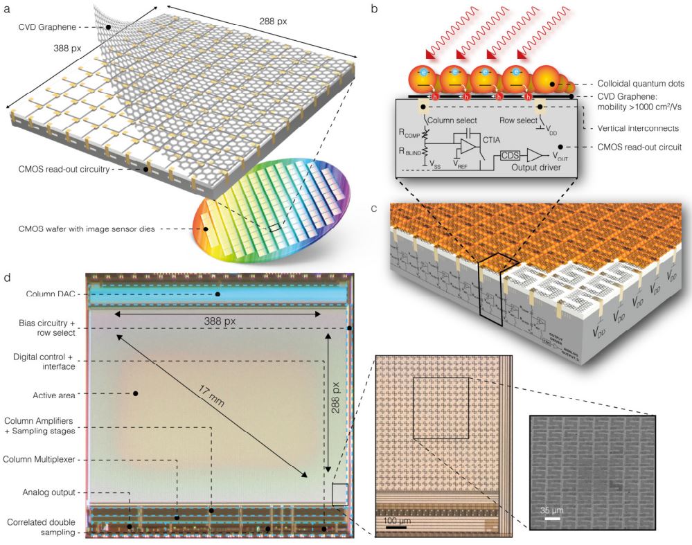
Image sensor array based on graphene-CMOS integration" by Stijn Goossens, Gabriele Navickaite, Carles Monasterio, Shuchi Gupta, Juan José Piqueras, Raúl Pérez, Gregory Burwell, Ivan Nikitskiy, Tania Lasanta, Teresa Galán, Eric Puma, Alba Centeno, Amaia Pesquera, Amaia Zurutuza, Gerasimos Konstantatos, and Frank Koppens. The authors are affiliated with Barcelona Institute of Science and Technology, Institució Catalana de Recerça, and Graphenea SA, all based in Spain.

From the abstract:

"Here, we show for the first time the monolithic integration of a CMOS integrated circuit with graphene, operating as a high mobility phototransistor. We demonstrate a high-resolution image sensor and operate it as a digital camera that is sensitive to UV, visible and infrared light (300 – 2000 nm). The demonstrated graphene-CMOS integration is pivotal for incorporating 2d materials into the next generation microelectronics, sensor arrays, low-power integrated photonics and CMOS imaging systems covering visible, infrared and even terahertz frequencies."

At a closer look, the sensing layer is, actually, "PbS colloidal quantum dots: upon light absorption an electron-hole pair is generated, due to the built in electric field the hole transfers to the graphene while the electron remains trapped in the quantum dots:"


"Due to the high mobility of graphene (here ~1000 cm2/Vs), this photoconductor structure exhibits ultra-high gain of 10^8 and responsivity above 10^7 A/W, which is a strong improvement compared to photodetectors and imaging systems based on quantum dots only."

The sample images are quite nice for a first graphene image sensor ever produced:


"Future graphene-based image sensors can be designed to operate at higher resolution, in a broader wavelength range, and potentially even with a form factor that fits inside a smartphone or smartwatch (Supplementary Notes, Figure S9). In contrast to current hybrid imaging technologies (which are not monolithic), we do not encounter fundamental limits with respect to shrinking the pixel size and increasing the imager resolution. Graphene patterning and contacting, i.e. lithography, will ultimately be the limiting factor. Therefore, competitively performing image sensors with multi-megapixel resolutions and pixel pitches down to 1 µm are within reach."

A somewhat similar paper, albeit from different authors, is going to be presented at ISSCC 2017 Session 15 on Feb. 7:

"15.7 Heterogeneous Integrated CMOS-Graphene Sensor Array for Dopamine Detection," B. Nasri, T. Wu, A. Alharbi, M. Gupta, R. Ranjit Kumar, S. Sebastian, Y. Wang, R. Kiani, D. Shahrjerdi, New York University, Brooklyn, NY.

Thursday, January 12, 2017

Corephotonics Raises $15M

Reuters, Globes: Israeli startup Corephotonics developing dual camera technologies for smartphones raises a $15M round bringing the total raised amount to $50M since it was founded in 2012.

The investors list in this round is impressive: Samsung Ventures, Foxconn, and MediaTek. Corephotonics’ current investors include Magma VC, Samsung Ventures, Amiti Ventures, Chinese billionaire Li Ka-shing and Solina Chau’s Horizon Ventures, OurCrowd, SanDisk, Chinese telephony services provider CK Telecom, and additional private investors.

The investment, along with the existing cash on hand and revenue forecast for 2017, will be used for developing next generation cameras for smartphones, and for expanding existing products’ penetration. In addition, the new funding will help Corephotonics expand into the automotive, drone, surveillance, and action camera markets.

Corephotonics, which currently has 50 employees, intends to recruit dozens of additional engineers for the company’s headquarters in Tel Aviv, as well as support and integration engineers in China and South Korea, following an expected significant growth in sales. In addition, the company is exploring opportunities to acquire complementary technologies.

The company co-founder and CEO David Mendelovic said, “We established Corephotonics in order to improve the image quality in smartphones, and to provide consumers with a unique user experience, after we identified this need of device manufacturers. We successfully predicted the use of dual cameras, and we currently see such cameras being integrated into a broad range of smartphones by all leading manufacturers. We are pleased that top tier investors have expressed confidence in our capabilities, allowing us to develop next generation camera technologies, which will reach the market within the next few years.

Corephotonics Hummingbird module

IISW 2017 Final Call for Papers

2017 International Image Sensor Workshop to be held on May 30 - June 2 2017 in Hiroshima, Japan announces Final Call for Papers and the Workshop registration details:

"Abstracts should be submitted electronically by January 19, 2017 (JST).

Registration is limited to approximately 160 attendees on a first-come, first-served basis. Registration will be guaranteed for presenters, but they are still required to register. Past experience shows that registration is often filled to capacity within a few days’ time.

Pre-registration will start on January 24, 2017 and end on February 10, 2017.

You will receive confirmation of your registration, and registration payment instructions, after all 160 attendees have been identified. It will be around February 20, 2017.
"

Grand Prince Hotel Hiroshima, IISW 2017 place

Wednesday, January 11, 2017

DxOMark Puzzled by Red Helium 8K Sensor Score

DxOMark publishes its scores for Red Helium 8K image sensor prototype, and tries to explain exceptionally high Raw performance of this APS-H sensor, even in comparison with Sony full-frame ones:


Puzzled by seemingly impossible improvements in SNR and DR over Sony BSI full-frame sensor, DxO checks Row files for pixel noise correlation, a sure sign of applied spatial noise reduction. However, there was no any correlation:


Then, DxO suspects that Red has applied a temporal noise reduction: "This technique, called temporal noise reduction (TNR), is most commonly used in video, since there are many successive frames to work with. However, temporal correlations across a time axis are not relevant when analyzing the image quality of a single RAW image, as they do not impact any RAW converters.

Whatever noise reduction system RED employs creating the RAW images from the Helium sensor, its presence means that we aren’t measuring just the RED sensor, so its results aren’t directly comparable to those from camera sensors we have tested from other vendors, whose RAW results come straight from the sensor with no prior noise reduction processing.
"

Apple AR Glasses Rumored to be Released in 2017

Forbes, CNET and other news sites quote veteran tech journalist Robert Scoble Facebook post claiming that "A Zeiss employee confirmed the rumors that Apple and Carl Zeiss AG are working on a light pair of augmented reality/mixed reality glasses that may be announced this year."

Few other bits of info originated from Robert Scoble, talking about 3D camera integration into Apple products:

"they are building the PrimeSense sensor right into the television, into the iPad and into the iPhone… so you can do this kind of mixed reality."

I interviewed the guy who runs PrimeSense and they have 600 engineers in Israel working on just the 3D sensor. What’s coming in 11 months is going to blow even my mind.

Apple Swift Head Becomes Tesla Autopilot SW Lead

Tesla welcomes Chris Lattner joining the company as VP of Autopilot Software. He comes to Tesla after 11 years at Apple where he was primarily responsible for creating Swift, the programming language for building apps on Apple platforms. Prior to Apple, Chris was lead author of the LLVM Compiler Infrastructure, an open source umbrella project that is widely used in commercial products and academic research today.

Tesla believes that the new appointment will accelerate the future of autonomous driving.

Huawei on Smartphone Camera Future

Image Sensors Europe conference publishes an interview with Atsushi Kobayashi, Senior Image Sensor Specialist from Huawei, talking about the future trends for smartphones. Few quotes:

"Most of key players like Huawei are eager to find out new camera feature and new key technology which improves camera performance.

Another area we are very excited about is ‘depth sensing’, especially due to the current demand for AR/VR applications. We anticipate in the next few years 3D cameras will become standard on all smart phones.

Improvements of pixel performance is still important, especially as Huawei is very open to new ideas which improves camera especially image sensor.
"

Tuesday, January 10, 2017

Canon on 250MP APS-H Sensor Plans

Imaging Resource publishes a PGN video interview with Canon representative at CES on how Canon plans to commercialize its 250MP CMOS sensor developed a few years ago:

Monday, January 09, 2017

IBM 5 in 5

IBM 5 in 5 - five innovations that IBM predicts will change our lives in the next five years - include, at least, two ones based on the image sensor technology:

- Hyperimaging - In five years, new imaging devices using hyperimaging technology and AI will help us see broadly beyond the domain of visible light by combining multiple bands of the electromagnetic spectrum to reveal valuable insights or potential dangers that would otherwise be unknown or hidden from view. Most importantly, these devices will be portable, affordable and accessible, so superhero vision can be part of our everyday experiences.


- Medical labs “on a chip” - In 5 years, new medical labs on a chip will serve as nanotechnology health detectives – tracing invisible clues in our bodily fluids and letting us know immediately if we have reason to see a doctor. The goal is to shrink down to a single silicon chip all of the processes necessary to analyze a disease that would normally be carried out in a full-scale biochemistry lab. Most of the sensing elements in these chips are similar to the pixel designs and based on the image sensor technology.

Augmented Reality Vanity Mirror

PRNewswire: Element Electronics, in partnership with FaceCake Marketing Technologies, debutes a NextGen AR vanity mirror, based on a camera inside:

"Most of us have been there. Wishing for a magic mirror that shows you what your makeup looks like before you apply it – potentially avoiding that dreaded lipstick or eye shadow mistake.

This traditional and sophisticated vanity mirror with adjustable LED lights and a sensor that accounts for the natural or artificial lighting conditions of the room can instantly transition into a personalized AR environment that lets consumers virtually see cosmetics and accessories – whether they own them or not – on their real-time reflection while receiving personalized recommendations and purchase options.
"