Aphesa comes up with a nice list of pixel defects:
Dead pixels do not respond to light at all and they don't provide any information. Dead pixels can be black, white (or let's say the maximum output value) or any intermediate value (also called stuck pixels).
Hot pixels respond do light normally but suffer from excessive dark current and can saturate at reasonable exposures even in the dark.
RTS pixels respond to light and provide once in a while a sequence of correct values but they can randomly jump up and down with a well defined offset. RTS also can be in a dark current where the dark current value randomly jumps between few discrete values.
Wide variance noise pixels have in average the right response to light but their noise is much larger than for the other pixels.
Blinking pixels can be either dead blinking if they jump randomly between two dead states or blinking operating if they jump between the right value and a dead state.
Clipping pixels behave normally up to a certain value (resp. from a certain value) where they will clip. They are only usable below (resp. above) their clipping value.
The pixels that start at a too high value sometimes only have excessive offset (can be caused by an excessive FD leakage, or memory node leakage in global shutter pixels.)
While the list is quite exhaustive and covers most of the known effects, there are few more that could be added:
Pixel with excessive image lag - can manifest itself as a non-linearity at low light. Can only appear at low temperatures. Depending on the array timing, can only appear in high frame rate modes.
Large crosstalk pixels - some pixels can suffer from too much coupling between them
Defective color response - can come from defects in color filter
Anomalously high or low photoresponse (too high PRNU) - can be caused by contamination particles masking a part of the light, or defects in metals, light pipes, etc.
Dark current that non-linearly depends on the integration time (for example, starts from high and getting lower after a couple of ms.)
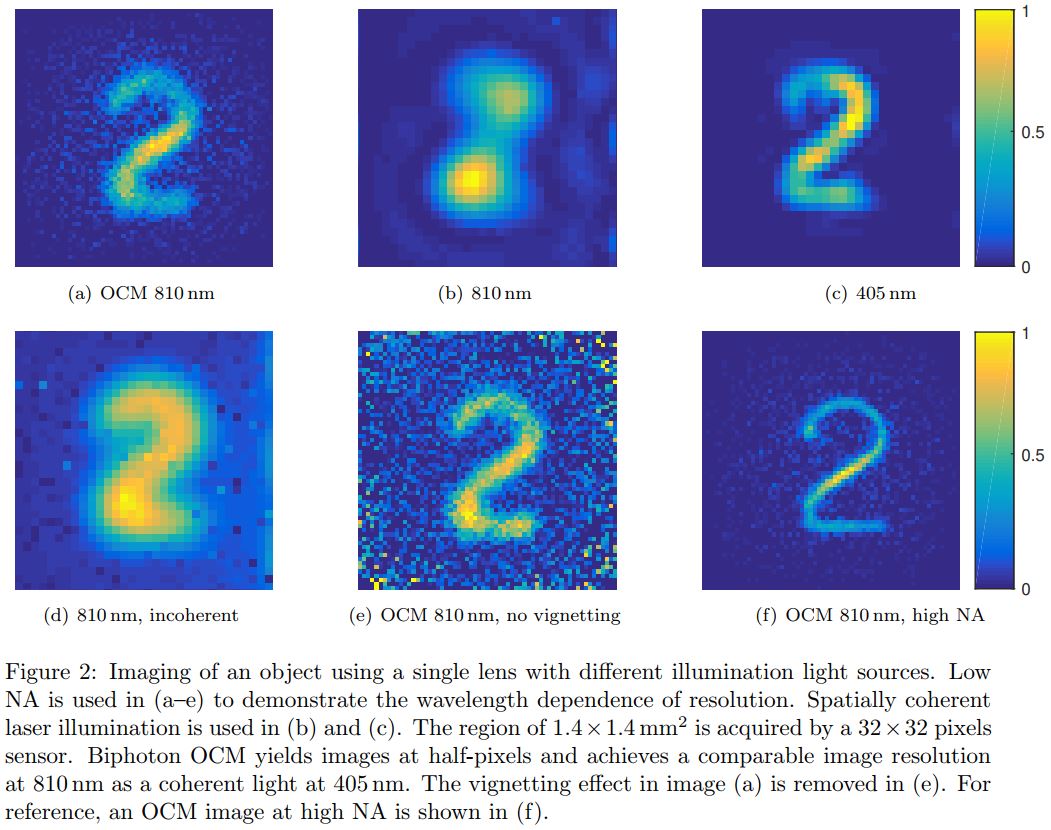
Arxiv.org paper "Super-Resolution Quantum Imaging at the Heisenberg Limit" by Manuel Unternährer, Bänz Bessire, Leonardo Gasparini, Matteo Perenzoni, and André Stefanov from FBK, Italy and Institute of Applied Physics, University of Bern, Switzerland combines an entangled photons light source and a single-photon imager to overcome diffraction resolution limit:
"Quantum imaging exploits the spatial correlations between photons to image object features with a higher resolution than a corresponding classical light source could achieve. Using a quantum correlated N-photon state, the method of optical centroid measurement (OCM) was shown to exhibit a resolution enhancement by improving the classical Rayleigh limit by a factor of 1/N. In this work, the theory of OCM is formulated within the framework of an imaging formalism and is implemented in an exemplary experiment by means of a conventional entangled photon pair source. The expected resolution enhancement of a factor of two is demonstrated. The here presented experiment allows for single-shot operation without scanning or iteration to reproduce the object in the image plane. Thereby, photon detection is performed with a newly developed integrated time-resolving detector array. Multi-photon interference effects responsible for the observed resolution enhancement are discussed and possible alternative implementation possibilities for higher photon number are proposed."
"In conclusion, our theoretical and experimental results demonstrate that quantum states of light showing super-resolution at the Heisenberg limit can be engineered. By limiting the Rayleigh resolution in low NA single-lens imaging, different light sources are compared in their ability to transmit spatial information. The OCM biphoton state used in our experiment shows a resolution enhancement close to a factor of two and is comparable to imaging at half the wavelength. For high NA systems, where the classical resolution is mainly limited by the wavelength, or for higher photon number N, theory suggests the possibility to have sub-wavelength image features present in the centroid coordinate. A full vectorial field analysis in contrast to the scalar approximations has yet to show the advantage in the limit of high NA.
Integrated single-photon detector arrays as presented here will certainly give rise to more experiments and applications in the field of quantum imaging. While the device in this work has non-optimal detection efficiency at the used wavelength, a speed up in acquisition time and higher photon number correlation measurement is expected in more optimized settings."
Japan Times reports that "Facial recognition technology will be used at the Tokyo 2020 Olympics and Paralympics to streamline the entry of athletes, officials and journalists to the games venues.
In light of concerns about terrorism, the games’ organizers aim to bolster security and prevent those involved in the 2020 Games from lending or borrowing ID cards.
The Justice Ministry deployed gates using facial recognition technology to screen passengers at Tokyo’s Haneda airport in October."
DailyMail reports about more cases of Apple Face ID false positive identifications in China.
Not only Apple face recognition system can fail. ZDNet reports that Germany-based SySS was able to trick some versions of Windows Hello on Surface Pro 4 equipped with an IR camera used by face recognition:
BLCV publishes a series of articles "Demystifying Face Recognition", currently 4 articles explaining everything from basics to more advanced computer learning aspects.
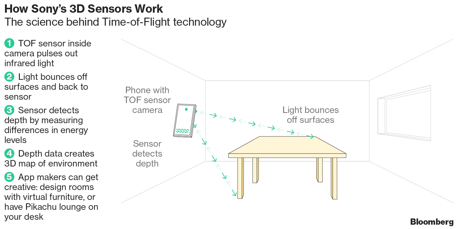
Bloomberg quotes Satoshi Yoshihara, GM of Sony image sensors division saying on 3D image sensing: "This has the scale to become the next pillar of our business."
"The most immediate impact from TOF sensors, which will be fabricated at Sony’s factories in Kyushu, will probably be seen in augmented-reality gadgets.
“Sony has everything technology-wise to address the market,” said Pierre Cambou, an imaging analyst at Yole. “They shouldn’t have a problem gaining a large share in 3D.”
When Sony decided to gamble on time-of-flight sensors three years ago, it faced a choice between building or buying the technology. In 2015, Sony decided to acquire Softkinetic Systems, a small developer of TOF sensors.
“When our engineers and their engineers talked about collaborating, we realized we could come up with an amazing sensor,” Yoshihara said of the merger. “In terms of both (chip) performance and size, we can achieve another breakthrough.”
Alexis Breton, a spokesman for STMicro, declined to comment, pointing to recent data showing that it’s shipped more than 300 million TOF chips. STMicro’s revenue from the division that mostly includes the sensors was $295 million last year."
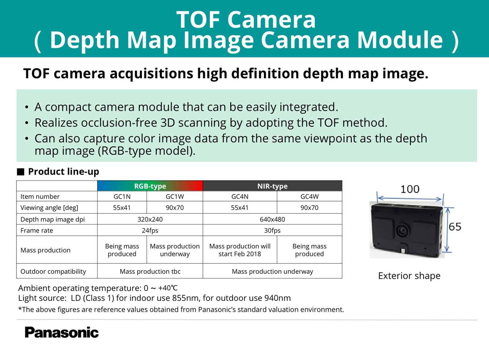
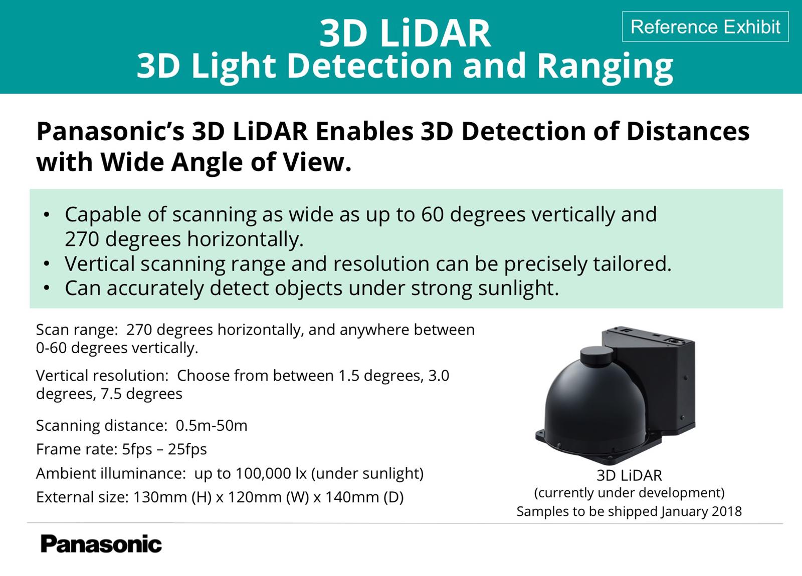
Panasonic too presents a number of 3D ToF cameras:
Basler uses Panasonic ToF sensors in its 3D cameras. The company's ToF products marketing manager Jana Bartels explains the camera features:
MIT Media Lab publishes a IEEE Access paper "Rethinking Machine Vision Time of Flight
With GHz Heterodyning" by Achuta Kadambi and Ramesh Raskar presenting "time-of-flight imaging that increases its depth resolution 1,000-fold. That’s the type of resolution that could make self-driving cars practical... At distances of 2 meters, the MIT researchers’ system... has a depth resolution of 3 micrometers."
The paper presents an indirect ToF imaging with a GHz modulation frequency:
Zurich, Switzerland-based Insightness uses its new event-driven Silicon Eye sensor and of pose estimation tracks from new EIVO tracking pipeline overlayed with APS images to draw Christmas tree.
- APS frame rate and rendering at 10Hz
- Pose estimation based on events
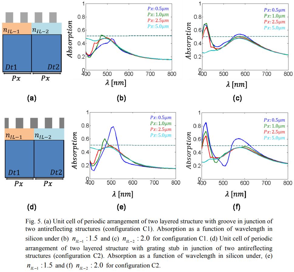
Optics Express publishes an open-access paper "Spectral sorting of visible light using dielectric gratings" by Ujwol Palanchoke, Salim Boutami, and Serge Gidon, Commissariat à l'Energie Atomique et aux Energies Alternatives, Grenoble, France. From the abstract:
"We show that by using grating structures, the spectral sorter structures are more efficient when the detector size is less than 1µm, enabling the shrinking of the detector size to the wavelength scale. A comprehensive design strategy is derived that could be used as a design guideline to achieve the sorting of visible light. We show that for pixel size as small as 0.5µm, optical efficiency as high as 80% could be achieved using dielectric based sorting structures."
"...the researchers show that the DiffuserCam can be used to reconstruct 100 million voxels, or 3D pixels, from a 1.3-megapixel (1.3 million pixels) image without any scanning.
...Although the hardware is simple, the software it uses to reconstruct high resolution 3D images is very complex.
The DiffuserCam is a relative of the light field camera, which captures how much light is striking a pixel on the image sensor as well as the angle from which the light hits that pixel.
Until now, light field cameras have been limited in spatial resolution because some spatial information is lost while collecting the directional information. Another drawback of these cameras is that the microlens arrays are expensive and must be customized for a particular camera or optical components used for imaging.
using random bumps in privacy glass stickers, Scotch tape or plastic conference badge holders, allowed the researchers to improve on traditional light field camera capabilities by using compressed sensing to avoid the typical loss of resolution that comes with microlens arrays.
Although other light field cameras use lens arrays that are precisely designed and aligned, the exact size and shape of the bumps in the new camera’s diffuser are unknown. This means that a few images of a moving point of light must be acquired to calibrate the software prior to imaging. The researchers are working on a way to eliminate this calibration step by using the raw data for calibration. They also want to improve the accuracy of the software and make the 3D reconstruction faster."
Sony Corp is poised to report its highest-ever profit this year on strong sales of image sensors after years of losing ground in consumer electronics and hopes to develop the technology for use in robotics and self-driving cars as competition heats up.
Executives say a technological breakthrough in image sensors and seachange in the company’s thinking are behind the success. The breakthrough, creating a sensor that captures more light to produce sharper images, coincided with soaring consumer demand for better smartphone cameras for sharing photos on social media.
The breakthrough, which involved reconfiguring the sensor layout and known as backside illumination, allowed Sony to grab nearly half of the market for image sensors.
“We knew we wouldn’t be able to win if we did what our rivals were doing,” said Teruo Hirayama, technology chief of Sony’s chip business, recalling initial scepticism around the technology that is now used widely.
“It was a great help for us to be told that we should operate independently,” Terushi Shimizu, the chief of Sony’s chip division, said, “rather than just belong to Sony.”
But the company is already bracing for intensifying competition in sensors as rivals, such as Samsung and OmniVision Technologies, step up their game, and is developing new sensor technologies for use in robotics and self-driving cars.
Investors say Sony still has a technological advantage that will take time for others to replicate.
“Sony has been trying to be ahead, but could face a turning point in a year or two,” said Kun Soo Lee, senior principal analyst with IHS Markit in Tokyo.
It is developing sensor technologies that can quickly measure distances or detect invisible light that are expected to be used in autonomous driving, factory automation and robotics, they said.
“It’s clear that we are currently dependent on the smartphone market,” Shimizu, the chip business chief said. “The market’s shift to dual-lens cameras from single-lens is good for us, but how long is this going to last as the market is only growing 1 or 2 percent?”
Terushi Shimizu, the chief of Sony’s chip division
Terushi Shimizu, the chief of Sony’s chip division
Teruo Hirayama, technology chief of Sony’s chip business
Magic Leap unveils its first AR product - Magic Leap One Creator Edition glasses. There is an impressive camera and vision technology integrated into the glasses:
Rolling Stone was given a chance to see Magic Leap demo and was generally positive about the new glasses performance.
Albert Theuwissen's IEEE webinar "Noise: You Love It or You Hate It" to be held on January 24, 2018 10:00am EST, will focus on the various noise sources present in a CMOS image sensor. A CMOS image sensor is a great example of a mixed-signal
circuit : the analog pixel array is driven by digital control signals. The analog output signal generated by the pixel array, goes through a denoising step in the analog domain before being converted to the digital domain. So it should not be surprising that a CMOS image sensor is a complex collection of different noise sources.
This webinar will address the most important noise sources in a CMOS image sensor, from temporal noise to spatial noise. The origin of those noise sources will be explained and countermeasures will be suggested. A lot of the countermeasures are already implemented in today's devices. Without the tremendous noise reduction techniques developed in the last decades, it would never ever have been possible to make color images at the extreme low light levels like we have at this moment. The noise floor of today's devices is that low that we can almost detect single electrons with standard consumer devices. Noise : do you love it or do you hate it? As a consumer I hate it, as an imaging engineer I love it! (These are Albert Theuwissen's words. As of me, I hate noise in any capacity.)
"A noteworthy twist on Bayer RGB is Samsung’s TetraCell and OmniVision’s 4-Cell strategy for high resolution front-facing cameras. This strategy enables in-pixel binning for greater sensitivity (with lower resolution) for low-lit scenes.
...as we end 2017 we are happy to announce we have found 0.9 µm generation pixels in mass production!
...we are tracking new types of associated autofocus (AF) systems, including: laser-assist, lossless phase detection autofocus (PDAF) in 1.0 µm telephoto camera chips, new types of masked PDAF, etc. Samsung is notable for its preference of a dual photodiode (Dual Pixel) AF system that is successful in its own right, and does not currently require laser-assist AF.
...we still primarily see TSV-based chip-to-chip interconnect, although Sony has been using direct bond interconnects (Cu-Cu hybrid bonding, or DBI) since early 2016. We recently saw OmniVision and foundry partner TSMC join the hybrid bonding club and claim the new world record, based on TechInsights’ findings, of 1.8 µm diameter, 3.7 µm pitch DBI pads.
...we’ve tracked in 2017 is the continued emergence of cameras with improved near infrared (NIR) sensitivity... We’re also analyzing the structures from new process flows in use, such as the pyramid surface diffraction structures on the SmartSens SC5035. Sony has previously announced a similar approach, and we expect a comparable structure in use for OmniVision’s announced Nyxel platform."
Samsung 0.9 µm ISOCELL Pixel with Tetracell Color Filters
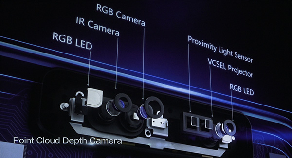
XDA Developers quotes Italian-language Notebook Italia info about Huawei "Point Cloud Depth Camera" based on an interview with one of Huawei engineers and the recent company presentation already mentioned in the previous post.
Here are the last few minutes from Huawei presentation in London:
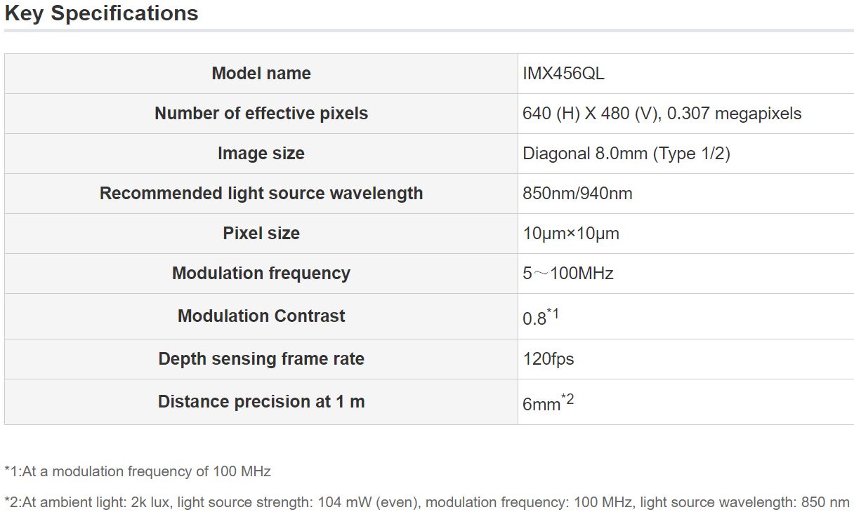
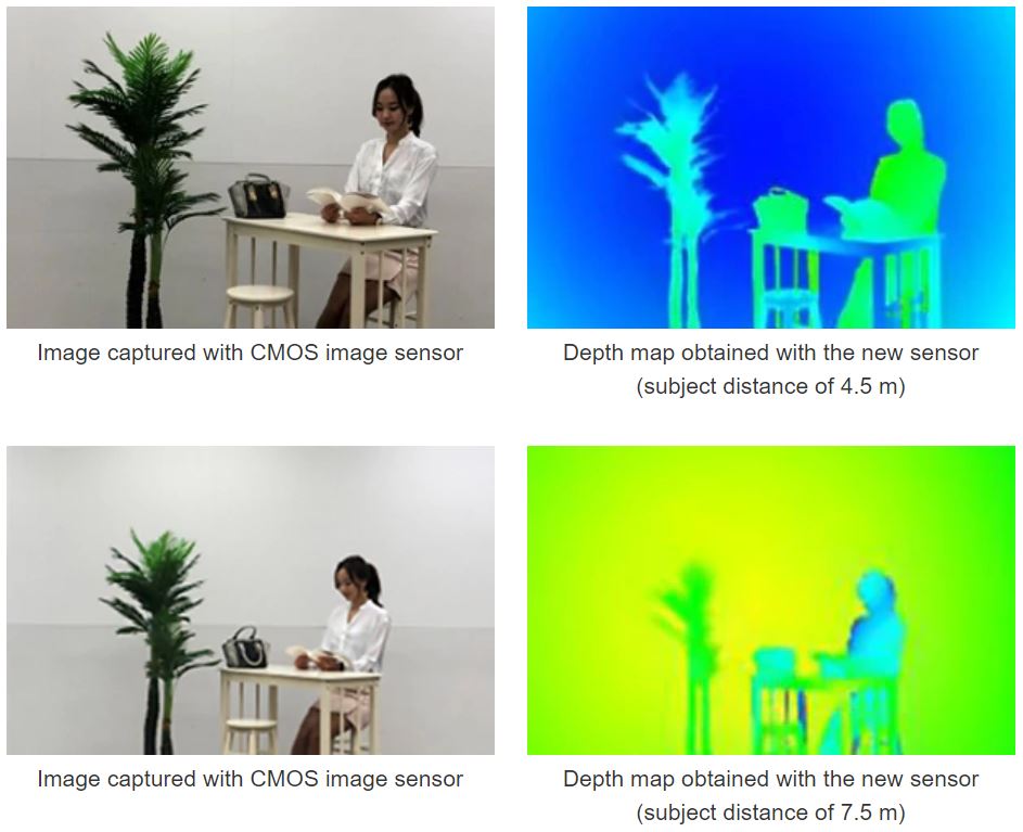
After announcing development of BSI ToF sensor half a year ago, Sony announces the release of 1/2-inch VGA IMX456QL product, with samples shipments planned for April 2018. The pixel size is about 10um.
"While conventional ToF sensor has difficulty in measuring far distance of approximately 10 meters, the new product comes with a sensitivity raising mode, enabling distance measurement with a high rate of detection at these distances. It is also possible to capture high-precision depth maps in a VGA resolution at close distances of approximately 30 centimeters to 1 meter.
Additionally, because this sensor captures depth maps for each frame, it enables image capture at a higher frame rate than when using a laser to scan the object for distance measurement. This reduces distortion of moving subjects in depth maps."
"This transition is the culmination of our work as a Sony subsidiary over the past couple of years," states Softkinetic CEO Akihiro Hasegawa. "We are honored of becoming an integral part of the world's leading image sensing company, and we will continue working towards the integration of our DepthSense technology into products for mobile, robotics, and automotive industries worldwide."
"We have great expectations for depth sensing technology," explains Sony Semiconductor Solutions Corporation Senior General Manager, Satoshi Yoshihara, "as we continue expanding the realm of senses for machines by enabling them with human-like sight."
A compelling achievement in this area has been the integration of DepthSense technology and gesture recognition software into premium vehicles and is the recent integration of DepthSense camera module and software designed by the Brussels-based company into Sony's new Entertainment Robot "aibo".
Espros December 2017 newsletter announces a tapeout of its pulsed LiDAR sensor:
"It is done! The design of the first LiDAR imager, or as we it call, pTOF imager is completed and the tapeout has happened a few days ago. The numbers are simply breath taking: The pixel has a sensitivity to recognize an object from 20 electrons only. This allows to detect an object in a 300m distance (white wall). A high performance 4-phase CCD with hundreds of gates operating at 250MHz clock does the time-to-location transformation. More than 10 million devices are placed on this chip. And more than 25 engineering man-years were squeezed into calendar year 2017. We are extremely proud on our chip design team for this outstanding achievement!"
ArsTechnica: Google announces that its AR project Tango with PMD ToF camera inside is officially shut down. ArsTechnica states the reasons for the discontinuation:
"Even with all the extra hardware, Tango's tracking was never that great. The constant drifting and other tracking errors made some of the coolest apps, like a measuring tape, unreliable for even small measurements. One amazing app, called "Matterport Scenes," turned the phone into a handheld 3D scanner, but the tracking errors meant your scans were never great at picking up detail. The app also absolutely crushed the Tango hardware and, after a few minutes of scanning things, would close with an out-of-memory error. Even games never really took off on the platform thanks to the low install base."
South China Morning Post reports that Chinese woman has been offered a refund after Apple Face ID allowed a colleague to unlock her iPhone X:
Meanwhile, a number of companies in China announce smartphones with Face Unlock: Vkworld S8, Vernee X and many others.
“We put an optical encoder between the lens and the image sensor, and it puts a time stamp on photons as they come in, so we can extract range information,” says Hal Zarem, chief executive of TetraVue.
That optical method has the advantage of scalability, which is why TetraVue’s system boasts 2 megapixels. And because the 100-nanosecond-long flashes repeat at a rate of 30 hertz, the lidar provides 60 million bits of data per second. That’s high-definition, full motion video.
“Because you get standard video as well as lidar for each pixel, you don’t have to figure which object the photon came from—it’s inherently fused in the camera,” says Zarem.
No other lidars will be needed, he adds. Translation: Say goodbye to all the other lidar companies you’ve heard about—Velodyne, for example. As for the other sensors, well, radars will survive, as will a few cameras to fill secondary roles such as showing what’s behind the car when you back up."
Tetravue official PR is here. The Tetravue LiDAR operation is explained here. TrafficTechnologyToday publishes a couple of Tetravue slides:
BusinessWire: Diabotics ports its LiDAR image processing software to Renesas R-Car platform:
"LiDAR processing today requires an efficient processing platform and advanced embedded software. By combining Renesas’ high-performance image processing, low-power automotive R-Car system-on-chip (SoC) with Dibotics’ 3D simultaneous localization and mapping (SLAM) technology, the companies deliver a SLAM on Chip™ (Note 1). The SLAM on Chip implements 3D SLAM processing on a SoC, a function that used to require a high-performance PC. It also realizes 3D mapping with LiDAR data only, eliminating the need to use inertial measurement units (IMUs) and global positioning system (GPS) data. The collaboration enables a real-time 3D mapping system with low power consumption and high-level functional safety in automotive systems.
Unlike existing approaches, Dibotics’ Augmented LiDAR™ software realizes 3D SLAM technology that only requires data from the LiDAR sensor to achieve 3D mapping. It does not require additional input from IMUs, GPS, or wheel encoders, which eliminates extra integration efforts, lowers bill-of-material (BOM) costs and simplifies development. In addition, the software realizes point-wise classification (Note 3), detection and tracking of shape, speed, and trajectory of moving objects, and Multi-LiDAR fusion."